 | –≠–ª–µ–∫—Ç—Ä–æ–Ω–Ω—ã–π –∫–æ–º–ø–æ–Ω–µ–Ω—Ç: M48T212A | –°–∫–∞—á–∞—Ç—å:  PDF PDF  ZIP ZIP |
1/20
PRELIMINARY DATA
March 2000
This is preliminary information on a new product now in development or undergoing evaluation. Details are subject to change without notice.
M48T212A
3.3V TIMEKEEPER
Æ
CONTROLLER
s
CONVERTS LOW POWER SRAM into
NVRAMs
s
YEAR 2000 COMPLIANT (4-Digit Year)
s
USES SUPER CAPACITOR or LITHIUM
BATTERY (User Supplied)
s
BATTERY LOW FLAG
s
INTEGRATED REAL TIME CLOCK,
POWER-FAIL CONTROL CIRCUIT
s
AUTOMATIC POWER-FAIL CHIP DESELECT
and WRITE PROTECTION
s
WATCHDOG TIMER
s
WRITE PROTECT VOLTAGES
(V
PFD
= Power-fail Deselect Voltage):
≠ M48T212A: 2.7V
V
PFD
3.0V
s
MICROPROCESSOR POWER-ON RESET
s
PROGRAMMABLE ALARM OUTPUT ACTIVE
in the BATTERY BACKED-UP MODE
DESCRIPTION
The M48T212A is a self-contained device that in-
cludes a real time clock (RTC), programmable
alarms, a watchdog timer, and two external chip
enable outputs which provide control of up to four
(two in parallel) external low-power static RAMs.
A built-in 32.768 kHz oscillator (external crystal
controlled) is used for the clock/calendar function.
Access to all TIMEKEEPER functions and the ex-
ternal RAM is the same as conventional byte-wide
SRAM. The 16 TIMEKEEPER Registers offer
Century, Year, Month, Date, Day, Hour, Minute,
Second, Control, Calibration, Alarm, Watchdog,
and Flags. Externally attached static RAMs are
controlled by the M48T212A via the E1
CON
and
E2
CON
signals (see Table 4).
Automatic backup and write protection for an ex-
ternal SRAM is provided through V
OUT
, E1
CON
and E2
CON
pins. (Users are urged to insure that
voltage specifications, for both the controller chip
and external SRAM chosen, are similar).
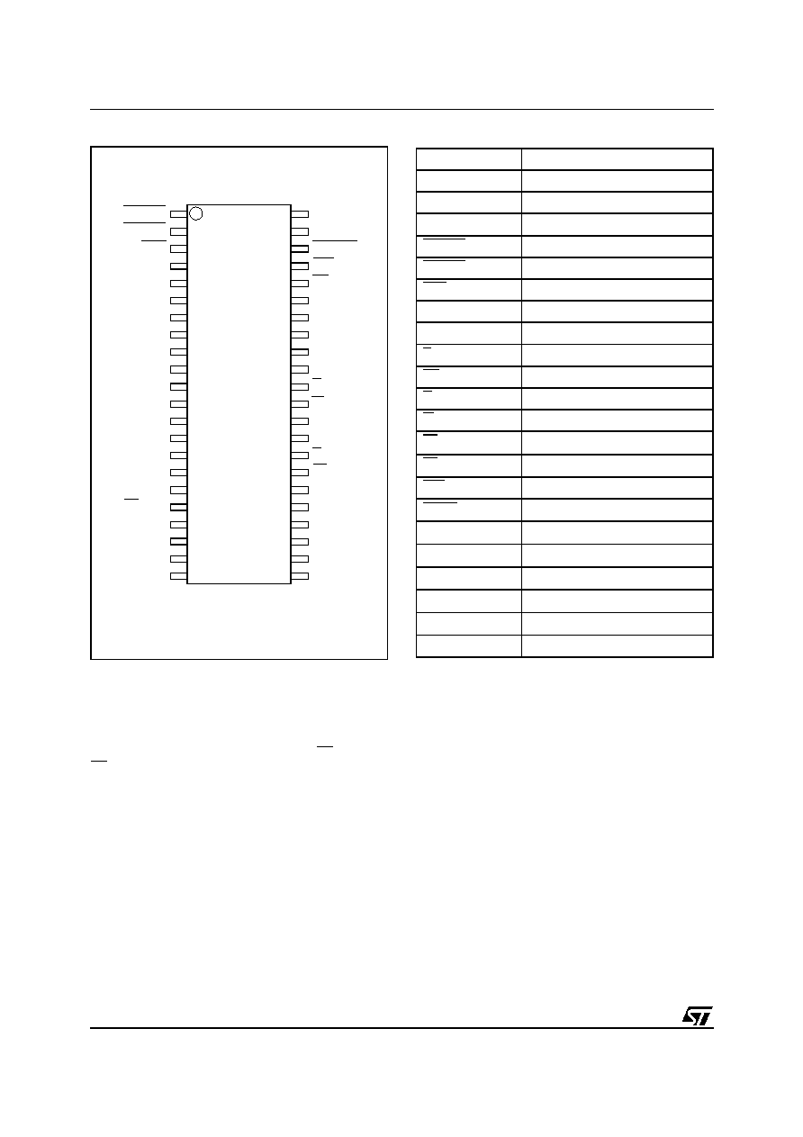
Figure 1. Logic Diagram
AI03047
4
A0-A3
A
DQ0-DQ7
VCC
M48T212A
G
VSS
8
EX
E2CON
E1CON
W
RSTIN2
RSTIN1
RST
IRQ/FT
VOUT
WDI
E
VCAP
X0
XI
VCCSW
VBAT≠
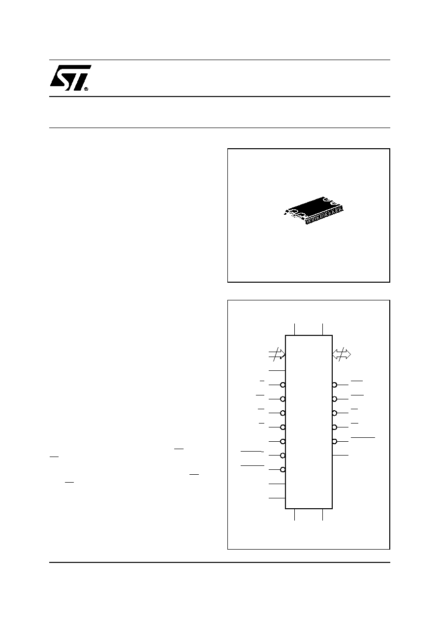
SOH44 (MH)
44
1
M48T212A
2/20
The lithium energy source (or super capacitor)
used to permanently power the real time clock is
also used to retain RAM data in the absence of
V
CC
power through the V
OUT
pin.
The chip enable outputs to RAM (E1
CON
and
E2
CON
) are controlled during power transients to
prevent data corruption. The date is automatically
adjusted for months with less than 31 days and
corrects for leap years. The internal watchdog tim-
er provides programmable alarm windows.
The nine clock bytes (Fh - 9h and 1h) are not the
actual clock counters, they are memory locations
consisting of BiPORT
TM
read/write memory cells
within the static RAM array. Clock circuitry up-
dates the clock bytes with current information once
per second. The information can be accessed by
the user in the same manner as any other location
in the static memory array.
Byte 8h is the clock control register. This byte con-
trols user access to the clock information and also
stores the clock calibration setting. Byte 7h con-
tains the watchdog timer setting. The watchdog
timer can generate either a reset or an interrupt,
depending on the state of the Watchdog Steering
bit (WDS). Bytes 6h-2h include bits that, when pro-
grammed, provide for clock alarm functionality.
Alarms are activated when the register content
matches the month, date, hours, minutes, and
seconds of the clock registers. Byte 1h contains
century information. Byte 0h contains additional
flag information pertaining to the watchdog timer,
alarm and battery status.
The M48T212A also has its own Power-Fail De-
tect circuit. This control circuitry constantly moni-
tors the supply voltage for an out of tolerance
condition. When V
CC
is out of tolerance, the circuit
write protects the TIMEKEEPER register data and
external SRAM, providing data security in the
midst of unpredictable system operation. As V
CC
falls, the control circuitry automatically switches to
the battery, maintaining data and clock operation
until valid power is restored.
Table 1. Signal Names
A0-A3
Address Inputs
DQ0-DQ7
Data Inputs/Outputs
XO
Oscillator Output
XI
Oscillator Input
RSTIN1
Reset 1 Input
RSTIN2
Reset 2 Input
RST
Reset Output (Open Drain)
WDI
Watchdog Input
A
Bank Select Input
E
Chip Enable Input
EX
External Chip Enable Input
G
Output Enable Input
W
Write Enable Input
E1
CON
RAM Chip Enable 1 Output
E2
CON
RAM Chip Enable 2 Output
IRQ/FT
Int/Freq Test Output (Open Drain)
Vccsw
V
CC
Switch Output
V
OUT
Supply Voltage Output
V
CAP
Super Capacitor Input
V
BAT≠
Battery Ground Pin (optional)
V
CC
Supply Voltage
V
SS
Ground
NC
Not Connected internally
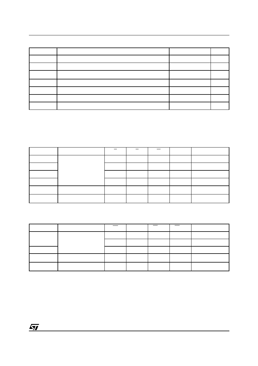
Figure 2. SOIC Connections
AI03048
22
44
43
VSS
1
A0
NC
NC
NC
A1
NC
A
NC
E1CON
NC
NC
VOUT
NC
G
E
VCC
M48T212A
10
2
5
6
7
8
9
11
12
13
14
15
21
40
39
36
35
34
33
32
31
30
29
28
XI
XO
EX
VCCSW
3
4
38
37
42
41
WDI
E2CON
DQ7
DQ5
DQ0
DQ1
DQ3
DQ4
DQ6
16
17
18
19
20
27
26
25
24
23
A2
A3
NC
RSTIN2
NC
RST
VCAP
NC
VBAT≠
W
NC
RSTIN1
DQ2
IRQ/FT
3/20
M48T212A
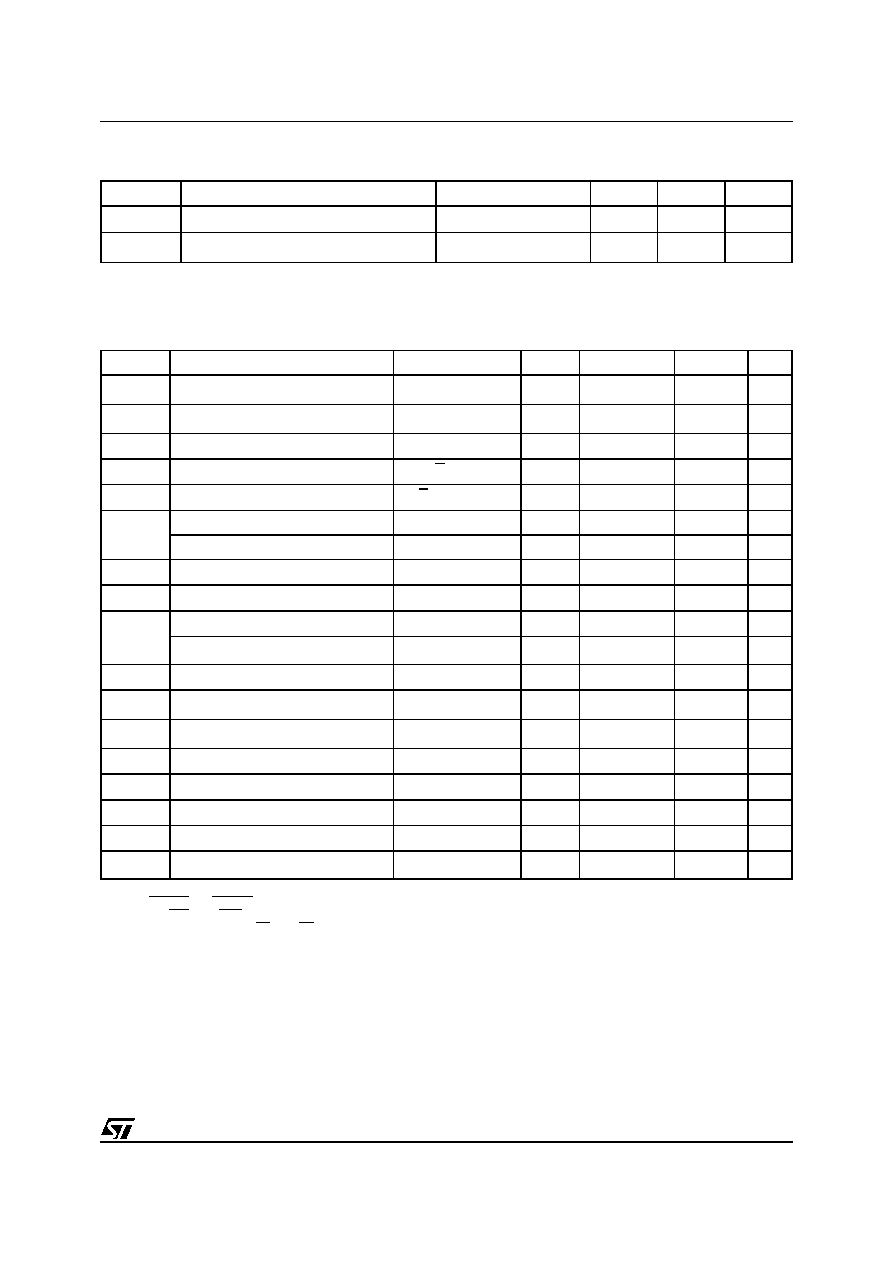
Table 2. Absolute Maximum Ratings
(1)
Note: 1. Stresses greater than those listed under "Absolute Maximum Ratings" may cause permanent damage to the device. This is a stress
rating only and functional operation of the device at these or any other conditions above those indicated in the operational section
of this specification is not implied. Exposure to the absolute maximum rating conditions for extended periods of time may affect
reliability.
2. Soldering temperature not to exceed 260∞C for 10 seconds (total thermal budget not to exceed 150∞C for longer than 30 seconds).
CAUTION: Negative undershoots below ≠0.3V are not allowed on any pin while in the Battery Back-up mode.
Table 3. Operating Modes
(1)
Note: 1. X = V
IH
or V
IL
.
2. V
SO
= Battery Back-up Switchover Voltage. (See Table 7 for details).
Table 4. Truth Table for SRAM Bank Select
(1)
Note: 1. X = V
IH
or V
IL
.
2. V
SO
= Battery Back-up Switchover Voltage. (See Table 7 for details).
Symbol
Parameter
Value
Unit
T
A
Ambient Operating Temperature
0 to 70
∞C
T
STG
Storage Temperature (V
CC
Off, Oscillator Off)
≠55 to 125
∞C
T
SLD
(2)
Lead Solder Temperature for 10 sec
260
∞C
V
IO
Input or Output Voltages
≠0.3 to 4.6
V
V
CC
Supply Voltage
≠0.3 to 4.6
V
I
O
Output Current
20
mA
P
D
Power Dissipation
1
W
Mode
V
CC
E
G
W
DQ7-DQ0
Power
Deselect
3.0V to 3.6V
V
IH
X
X
High-Z
Standby
Write
V
IL
X
V
IL
D
IN
Active
Read
V
IL
V
IL
V
IH
D
OUT
Active
Read
V
IL
V
IH
V
IH
High-Z
Active
Deselect
V
SO
to V
PFD
(min)
(2)
X
X
X
High-Z
CMOS Standby
Deselect
V
SO
(2)
X
X
X
High-Z
Battery Back-Up
Mode
V
CC
EX
A
E1
CON
E2
CON
Power
Select
3.0V to 3.6V
Low
Low
Low
High
Active
Low
High
High
Low
Active
Deselect
High
X
High
High
Standby
Deselect
V
SO
to V
PFD
(min)
(2)
X
X
High
High
CMOS Standby
Deselect
V
SO
(2)
X
X
High
High
Battery Back-Up
M48T212A
4/20
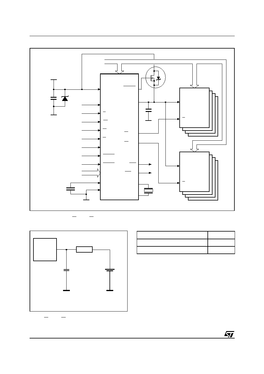
Figure 3. Hardware Hookup
Note: 1. See description in Power Supply Decoupling and Undershoot Protection.
2. Traces connecting E1
CON
and E2
CON
to external SRAM should be as short as possible.
AI03049
A0-A3
DQ0-DQ7
A
VCC
W
G
WDI
RSTIN1
RSTIN2
VCAP
E
VCC
A0-Axx
0.1
µ
F
0.1
µ
F
3.3V
E2CON
RST
IRQ/FT
M48T212A
CMOS
SRAM
VOUT
E1CON
Note 2
MOTOROLA
MTD20P06HDL
VCCSW
1N5817
(1)
EX
E
A0-A18
E
VCC
CMOS
SRAM
VSS
SuperCap Supply
A0-Axx
X0
XI
32 kHz
Crystal
Figure 4. AC Testing Load Circuit
(3,4)
Note: 1. DQ0-DQ7
2. E1
CON
and E2
CON
3. Excluding open-drain output pins
AI03239
CL = 100pF or 5pF
(1)
CL = 30 pF
(2)
645
DEVICE
UNDER
TEST
1.75V
CL includes JIG capacitance
Table 5. AC Measurement Conditions
Note that Output Hi-Z is defined as the point where data
is no longer driven.
Input Rise and Fall Times
5ns
Input Pulse Voltages
0 to 3V
Input and Output Timing Ref. Voltages
1.5V
5/20
M48T212A
Table 6. Capacitance
(1)
(T
A
= 25 ∞C, f = 1 MHz)
Note: 1. Sampled only, not 100% tested.
2. Outputs deselected.
Table 7. DC Characteristics
(T
A
= 0 to 70∞C; V
CC
= 3V to 3.6V)
Note: 1. Outputs deselected.
2. RSTIN1 and RSTIN2 internally pulled-up to V
CC
through 100K
resistor. WDI internally pulled-down to V
SS
through 100K
resistor.
3. For IRQ/FT & RST pins (Open Drain).
4. Conditioned outputs (E1
CON
- E2
CON
) can only sustain CMOS leakage currents in the battery back-up mode. Higher leakage cur-
rents will reduce battery life.
5. External SRAM must match TIMEKEEPER Controller chip V
CC
specification.
6. When fully charged.
Symbol
Parameter
Test Condition
Min
Max
Unit
C
IN
Input Capacitance
V
IN
= 0V
10
pF
C
OUT
(2)
Input/Output Capacitance
V
OUT
= 0V
10
pF
Symbol
Parameter
Test Condition
Min
Typ
Max
Unit
I
LI
(1,2)
Input Leakage Current
0V
V
IN
V
CC
±1
µA
I
LO
(1)
Output Leakage Current
0V
V
OUT
V
CC
±1
µA
I
CC
Supply Current
Outputs Open
4
10
mA
I
CC1
Supply Current (Standby) TTL
E = V
IH
3
mA
I
CC2
Supply Current (Standby) CMOS
E = V
CC
≠0.2
2
mA
I
BAT
Battery Current OSC ON
575
800
nA
Battery Current OSC OFF
100
nA
V
IL
Input Low Voltage
≠0.3
0.8
V
V
IH
Input High Voltage
2.0
V
CC
+ 0.3
V
V
OL
Output Low Voltage
I
OL
= 2.1mA
0.4
V
Output Low Voltage (open drain)
(3)
I
OL
= 10mA
0.4
V
V
OH
Output High Voltage
I
OH
= ≠1.0mA
2.4
V
V
OHB
(4)
V
OH
Battery Back-up
I
OUT2
= ≠1.0µA
2.0
3.6
V
I
OUT1
(5)
V
OUT
Current (Active)
V
OUT1
> V
CC
≠0.3
70
mA
I
OUT2
V
OUT
Current (Battery Back-up)
V
OUT2
> V
BAT
≠0.3
100
µA
V
PFD
Power-fail Deselect Voltage
2.7
2.9
3.0
V
V
SO
Battery Back-up Switchover Voltage
V
PFD
≠100mV
V
V
BAT
Battery Voltage
3.0
V
V
CAP
Capacitor Voltage
(6)
V
CC
V