1/23
April 2000
M48T212Y
M48T212V
5V/3.3V TIMEKEEPER
Æ
CONTROLLER
s
CONVERTS LOW POWER SRAM into
NVRAMs
s
YEAR 2000 COMPLIANT (4-Digit Year)
s
BATTERY LOW FLAG
s
INTEGRATED REAL TIME CLOCK,
POWER-FAIL CONTROL CIRCUIT, BATTERY
and CRYSTAL
s
AUTOMATIC POWER-FAIL CHIP DESELECT
and WRITE PROTECTION
s
WATCHDOG TIMER
s
CHOICE of WRITE PROTECT VOLTAGES
(V
PFD
= Power-fail Deselect Voltage):
≠ M48T212Y: 4.2V
V
PFD
4.5V
≠ M48T212V: 2.7V
V
PFD
3.0V
s
MICROPROCESSOR POWER-ON RESET
s
PROGRAMMABLE ALARM OUTPUT ACTIVE
in the BATTERY BACKED-UP MODE
s
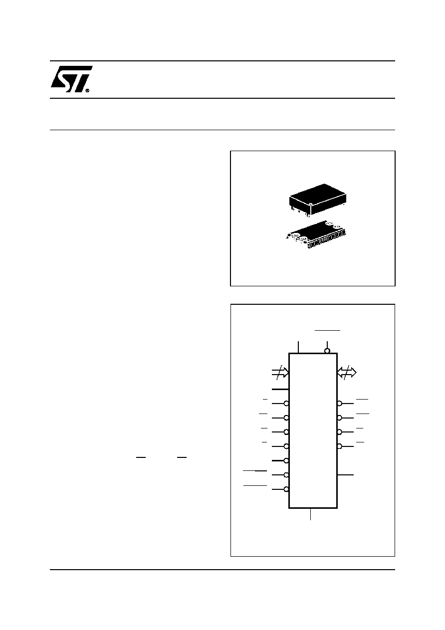
PACKAGING INCLUDES a 44-LEAD SOIC and
SNAPHAT
Æ
TOP (to be Ordered Separately)
DESCRIPTION
The M48T212Y/V are self-contained devices that
include a real time clock (RTC), programmable
alarms, a watchdog timer, and two external chip
enable outputs which provide control of up to four
(two in parallel) external low-power static RAMs.
Access to all TIMEKEEPER
Æ
functions and the
external RAM is the same as conventional byte-
wide SRAM. The 16 TIMEKEEPER Registers offer
Century, Year, Month, Date, Day, Hour, Minute,
Second, Calibration, Alarm, Watchdog, and Flags.
Externally attached static RAMs are controlled by
the M48T212Y/V via the E1
CON
and E2
CON
sig-
nals (see Table 4).
The 44 pin 330mil SOIC provides sockets with
gold plated contacts at both ends for direct con-
nection to a separate SNAPHAT housing contain-
ing the battery and crystal. The unique design
allows the SNAPHAT battery package to be
mounted on top of the SOIC package after the
completion of the surface mount process.
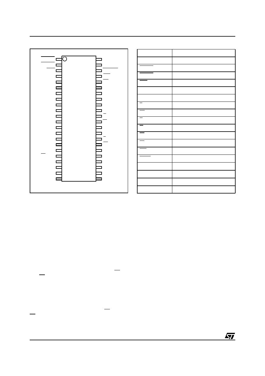
Figure 1. Logic Diagram
AI03019
4
A0-A3
A
DQ0-DQ7
VCC
M48T212Y
M48T212V
G
VSS
8
EX
E2CON
E1CON
W
RSTIN2
RSTIN1
RST
IRQ/FT
VOUT
WDI
E
VCCSW
SOH44 (MH)
SNAPHAT (SH)
Battery
44
1
M48T212Y, M48T212V
2/23
Insertion of the SNAPHAT housing after reflow
prevents potential battery and crystal damage due
to the high temperatures required for device sur-
face-mounting. The SNAPHAT housing is keyed
to prevent reverse insertion.
The SOIC and battery/crystal packages are
shipped separately in plastic anti-static tubes or in
Tape & Reel form. For the 44 lead SOIC, the bat-
tery/crystal package (i.e. SNAPHAT) part number
is "M4TXX-BR12SH" (see Table 15).
Caution: Do not place the SNAPHAT battery/crys-
tal top in conductive foam, as this will drain the lith-
ium button-cell battery.
Automatic backup and write protection for an ex-
ternal SRAM is provided through V
OUT
, E1
CON
and E2
CON
pins. (Users are urged to insure that
voltage specifications, for both the controller chip
and external SRAM chosen, are similar). The
SNAPHAT containing the lithium energy source
used to permanently power the real time clock is
also used to retain RAM data in the absence of
V
CC
power through the V
OUT
pin.
The chip enable outputs to RAM (E1
CON
and
E2
CON
) are controlled during power transients to
prevent data corruption. The date is automatically
adjusted for months with less than 31 days and
corrects for leap years. The internal watchdog tim-
er provides programmable alarm windows.
The nine clock bytes (Fh - 9h and 1h) are not the
actual clock counters, they are memory locations
consisting of BiPORT
TM
read/write memory cells
within the static RAM array. Clock circuitry up-
dates the clock bytes with current information once
per second. The information can be accessed by
the user in the same manner as any other location
in the static memory array.
Byte 8h is the clock control register. This byte con-
trols user access to the clock information and also
stores the clock calibration setting. Byte 7h con-
tains the watchdog timer setting. The watchdog
timer can generate either a reset or an interrupt,
depending on the state of the Watchdog Steering
bit (WDS). Bytes 6h-2h include bits that, when pro-
grammed, provide for clock alarm functionality.
Alarms are activated when the register content
matches the month, date, hours, minutes, and
seconds of the clock registers. Byte 1h contains
century information. Byte 0h contains additional
flag information pertaining to the watchdog timer,
alarm and battery status.
Table 1. Signal Names
A0-A3
Address Inputs
DQ0-DQ7
Data Inputs/Outputs
RSTIN1
Reset 1 Input
RSTIN2
Reset 2 Input
RST
Reset Output (Open Drain)
WDI
Watchdog Input
A
Bank Select Input
E
Chip Enable Input
EX
External Chip Enable Input
G
Output Enable Input
W
Write Enable Input
E1
CON
RAM Chip Enable 1 Output
E2
CON
RAM Chip Enable 2 Output
IRQ/F T
Int/Freq Test Output (Open Drain)
Vccsw
V
CC
Switch Output
V
OUT
Supply Voltage Output
V
CC
Supply Voltage
V
SS
Ground
NC
Not Connected internally
Figure 2. SOIC Connections
AI03020
22
44
43
VSS
1
A0
NC
NC
NC
A1
NC
A
NC
E1CON
NC
NC
VOUT
NC
G
E
VCC
M48T212Y
M48T212V
10
2
5
6
7
8
9
11
12
13
14
15
21
40
39
36
35
34
33
32
31
30
29
28
NC
NC
EX
VCCSW
3
4
38
37
42
41
WDI
E2CON
DQ7
DQ5
DQ0
DQ1
DQ3
DQ4
DQ6
16
17
18
19
20
27
26
25
24
23
A2
A3
NC
RSTIN2
NC
RST
NC
NC
NC
W
NC
RSTIN1
DQ2
IRQ/FT
3/23
M48T212Y, M48T212V
Table 2. Absolute Maximum Ratings
(1)
Note: 1. Stresses greater than those listed under "Absolute Maximum Ratings" may cause permanent damage to the device. This is a stress
rating only and functional operation of the device at these or any other conditions above those indicated in the operational section
of this specification is not implied. Exposure to the absolute maximum rating conditions for extended periods of time may affect
reliability.
2. Soldering temperature not to exceed 260
∞
C for 10 seconds (total thermal budget not to exceed 150
∞
C for longer than 30 seconds).
CAUTION: Negative undershoots below ≠0.3V are not allowed on any pin while in the Battery Back-up mode.
CAUTION: Do NOT wave solder SOIC to avoid damaging SNAPH AT sockets.
Table 3. Operating Modes
(1)
Note: 1. X = V
IH
or V
IL
.
2. V
SO
= Battery Back-up Swit chover Voltage. (See Tables 7A and 7B for details).
Table 4. Truth Table for SRAM Bank Select
(1)
Note: 1. X = V
IH
or V
IL
.
2. V
SO
= Battery Back-up Swit chover Voltage. (See Tables 7A and 7B for details).
Symbol
Parameter
Value
Unit
T
A
Ambient Operating Temperature
0 to 70
∞
C
T
STG
Storage Temperature (V
CC
Off, Oscillator Off)
SNAPHAT
SOIC
≠40 to 85
≠55 to 125
∞
C
T
SLD
(2)
Lead Solder Temperature for 10 sec
260
∞
C
V
IO
Input or Output Voltages
≠0.3 to V
CC
+0.3
V
V
CC
Supply Voltage
M48T212Y
M48T212V
≠0.3 to 7
≠0.3 to 4.6
V
I
O
Output Current
20
mA
P
D
Power Dissipation
1
W
Mode
V
CC
E
G
W
DQ7-DQ0
Power
Deselect
4.5V to 5.5V
or
3.0V to 3.6V
V
IH
X
X
High-Z
Standby
Write
V
IL
X
V
IL
D
IN
Active
Read
V
IL
V
IL
V
IH
D
OUT
Active
Read
V
IL
V
IH
V
IH
High-Z
Active
Deselect
V
SO
to V
PFD
(min)
(2)
X
X
X
High-Z
CMOS Standby
Deselect
V
SO
(2)
X
X
X
High-Z
Battery Back-Up
Mode
V
CC
EX
A
E1
CON
E2
CON
Power
Select
4.5V to 5.5V
or
3.0V to 3.6V
Low
Low
Low
High
Active
Low
High
High
Low
Active
Deselect
High
X
High
High
Standby
Deselect
V
SO
to V
PFD
(min)
(2)
X
X
High
High
CMOS Standby
Deselect
V
SO
(2)
X
X
High
High
Battery Back-Up
M48T212Y, M48T212V
4/23
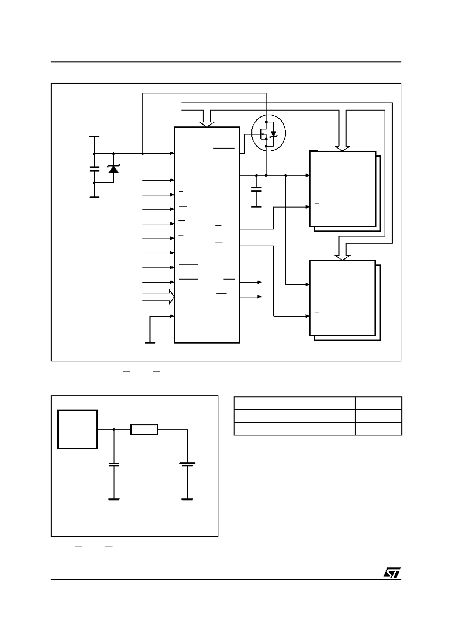
Figure 3. Hardware Hookup
Note: 1. See description in Power Supply Decoupling and Undershoot Protection.
2. Traces connecting E1
CON
and E2
CON
to external SRAM should be as short as possible.
AI03046
A0-A3
DQ0-DQ7
A
VCC
W
G
WDI
RSTIN1
RSTIN2
VSS
E
VCC
A0-Axx
0.1
µ
F
0.1
µ
F
5V/3.3V
E2CON
RST
IRQ/FT
M48T212Y/V
CMOS
SRAM
VOUT
E
VCC
CMOS
SRAM
E1CON
Note 2
MOTOROLA
MTD20P06HDL
VCCSW
1N5817
(1)
EX
E
A0-A18
A0-Axx
Figure 4. AC Testing Load Circuit
Note: 1. DQ0-DQ7
2. E1
CON
and E2
CON
AI03239
CL = 100pF or 5pF
(1)
CL = 30 pF
(2)
645
DEVICE
UNDER
TEST
1.75V
CL includes JIG capacitance
Table 5. AC Measurement Conditions
Note that Output Hi-Z is defined as the point where data
is no longer driven.
Input Rise and Fall Times
5ns
Input Pulse Voltages
0 to 3V
Input and Output Timing Ref. Voltages
1.5V
5/23
M48T212Y, M48T212V
Table 6. Capacitance
(1)
(T
A
= 25
∞
C, f = 1 MHz)
Note: 1. Sampled only, not 100% tested.
2. Outputs deselected.
Table 7A. DC Characteristics for M48T212V
(T
A
= 0 to 70
∞
C; V
CC
= 3V to 3.6V)
Note: 1. Outputs deselected.
2. RSTIN1 and RSTIN2 internally pulled-up to V
CC
through 100K
resistor. WDI internally pulled-down to V
SS
through 100K
resistor.
3. For IRQ/FT & RST pins (Open Drain).
4. Conditioned outputs (E1
CON
- E2
CON
) can only sustain CMOS leakage currents in the battery back-up mode. Higher leakage cur-
rents will reduce battery life.
5. External SRAM must match TIMEKEE PER Controller chip V
CC
specification.
Symbol
Parameter
Test Condit ion
Min
Max
Unit
C
IN
Input Capacitance
V
IN
= 0V
10
pF
C
OUT
(2)
Input/Output Capacitance
V
OUT
= 0V
10
pF
Symbol
Parameter
Test Condition
Min
Typ
Max
Unit
I
LI
(1,2)
Input Leakage Current
0V
V
IN
V
CC
±
1
µ
A
I
LO
(1)
Output Leakage Current
0V
V
OUT
V
CC
±
1
µ
A
I
CC
Supply Current
Outputs open
4
10
mA
I
CC1
Supply Current (Standby) TTL
E = V
IH
3
mA
I
CC2
Supply Current (Standby) CMOS
E = V
CC
≠0.2
2
mA
I
BAT
Battery Current OSC ON
575
800
nA
Battery Current OSC OFF
100
nA
V
IL
Input Low Voltage
≠0.3
0.8
V
V
IH
Input High Voltage
2.0
V
CC
+ 0.3
V
V
OL
Output Low Voltage
I
OL
= 2.1mA
0.4
V
Output Low Voltage (open drain)
(3)
I
OL
= 10mA
0.4
V
V
OH
Output High Voltage
I
OH
= ≠1.0mA
2.4
V
V
OHB
(4)
V
OH
Battery Back-up
I
OUT2
= ≠1.0
µ
A
2.0
3.6
V
I
OUT1
(5)
V
OUT
Current (Active)
V
OUT1
> V
CC
≠0.3
70
mA
I
OUT2
V
OUT
Current (Battery Back-up)
V
OUT2
> V
BAT
≠0.3
100
µ
A
V
PFD
Power-fail Deselect Voltage
2.7
2.9
3.0
V
V
SO
Battery Back-up Switchover Voltage
V
PFD
≠100mV
V
V
BAT
Battery Voltage
3.0
V