1/24
May 2003
Rev. 2.0
M48T254V
3.3V, 16 Mbit (2 Mb x 8 bit) TIMEKEEPER
Æ
SRAM WITH PHANTOM CLOCK
FEATURES SUMMARY
s
3.3V ± 10%
s
INTEGRATED ULTRA LOW POWER SRAM,
REAL TIME CLOCK, POWER-FAIL CONTROL
CIRCUIT, BATTERY AND CRYSTAL
s
REAL TIME CLOCK KEEPS TRACK OF
TENTHS/HUNDREDTHS OF SECONDS,
SECONDS, MINUTES, HOURS, DAYS, DATE,
MONTHS, and YEARS.
s
CLOCK FUNCTION IS TRANSPARENT TO
RAM OPERATION.
s
PRECISION POWER MONITORING and
POWER SWITCHING CIRCUITRY
s
AUTOMATIC WRITE-PROTECTION WHEN
V
CC
IS OUT-OF-TOLERANCE
s
POWER-FAIL DESELECT VOLTAGE:
≠ V
CC
= 3.3V ± 10%; 2.8V
V
PFD
2.97V
s
BATTERY LOW (BL)
s
10 YEARS of DATA RETENTION and CLOCK
OPERATION IN THE ABSENCE OF POWER
s
SNAPHAT HOUSING (BATTERY/CRYSTAL)
IS REPLACEABLE
s
100ns ACCESS (READ = WRITE)
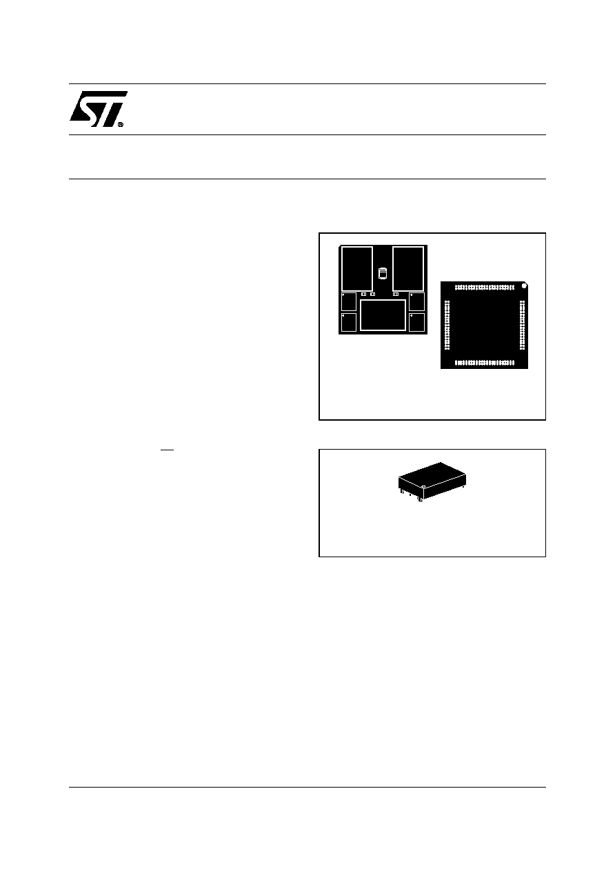
Figure 1. 168-ball PBGA Module
Figure 2. SNAPHAT Crystal/Battery
M48T254V
168-ball PBGA
Module (ZA)
SNAPHAT (SH)
Crystal/Battery

M48T254V
2/24
TABLE OF CONTENTS
SUMMARY DESCRIPTION . . . . . . . . . . . . . . . . . . . . . . . . . . . . . . . . . . . . . . . . . . . . . . . . . . . . . . . . . . . 3
Figure 3. Logic Diagram . . . . . . . . . . . . . . . . . . . . . . . . . . . . . . . . . . . . . . . . . . . . . . . . . . . . . . . . . . 3
Table 1. Signal Names . . . . . . . . . . . . . . . . . . . . . . . . . . . . . . . . . . . . . . . . . . . . . . . . . . . . . . . . . . . 3
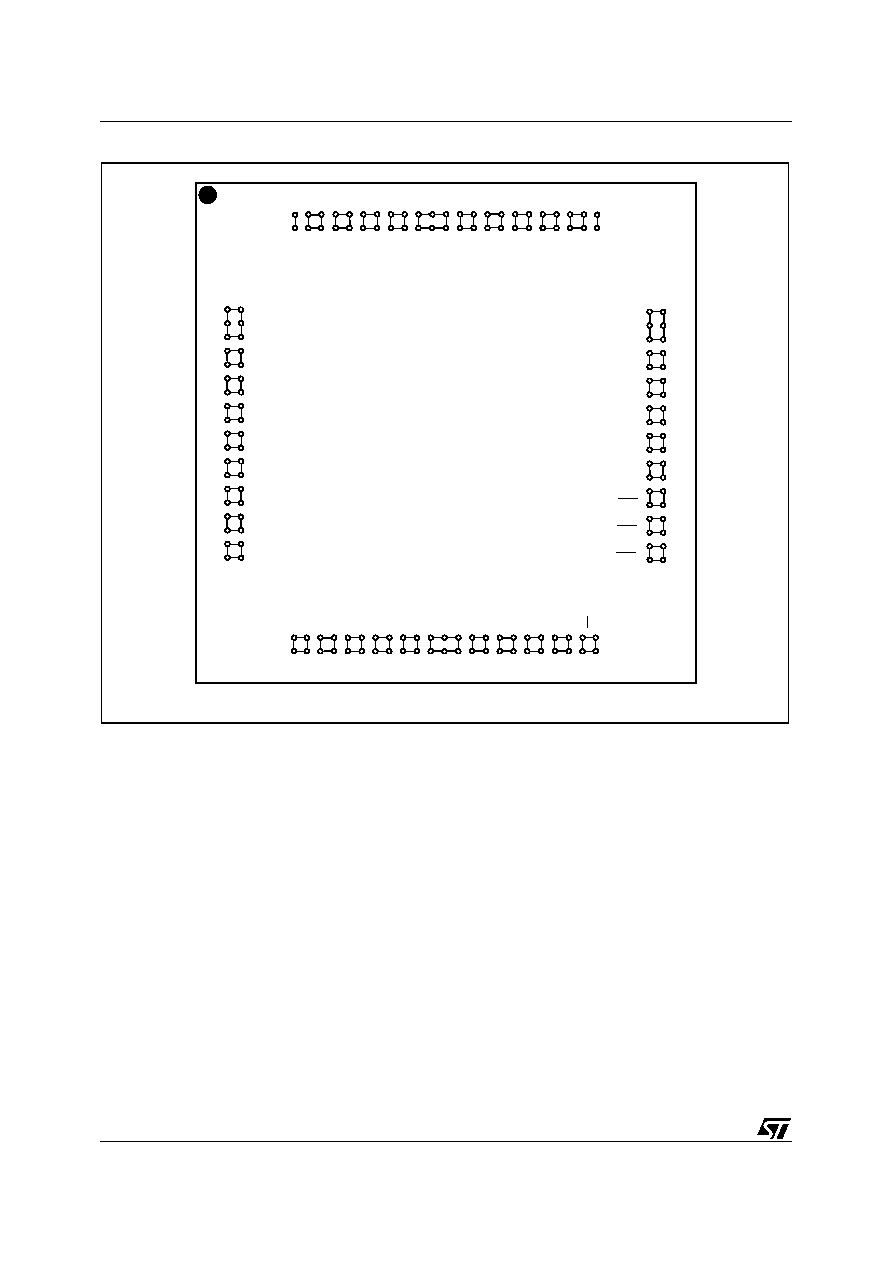
Figure 4. PBGA Connections (Top View) . . . . . . . . . . . . . . . . . . . . . . . . . . . . . . . . . . . . . . . . . . . . . 4
Figure 5. Hardware Hookup . . . . . . . . . . . . . . . . . . . . . . . . . . . . . . . . . . . . . . . . . . . . . . . . . . . . . . . 5
Figure 6. M48T254V PBGA Module Solution (Side/Top) . . . . . . . . . . . . . . . . . . . . . . . . . . . . . . . . . 6
MAXIMUM RATING. . . . . . . . . . . . . . . . . . . . . . . . . . . . . . . . . . . . . . . . . . . . . . . . . . . . . . . . . . . . . . . . . 6
Table 2. Absolute Maximum Ratings . . . . . . . . . . . . . . . . . . . . . . . . . . . . . . . . . . . . . . . . . . . . . . . . . 6
DC AND AC PARAMETERS. . . . . . . . . . . . . . . . . . . . . . . . . . . . . . . . . . . . . . . . . . . . . . . . . . . . . . . . . . 7
Table 3. DC and AC Measurement Conditions . . . . . . . . . . . . . . . . . . . . . . . . . . . . . . . . . . . . . . . . . 7
Figure 7. AC Testing Load Circuit . . . . . . . . . . . . . . . . . . . . . . . . . . . . . . . . . . . . . . . . . . . . . . . . . . . 7
Table 4. Capacitance. . . . . . . . . . . . . . . . . . . . . . . . . . . . . . . . . . . . . . . . . . . . . . . . . . . . . . . . . . . . . 7
Table 5. DC Characteristics. . . . . . . . . . . . . . . . . . . . . . . . . . . . . . . . . . . . . . . . . . . . . . . . . . . . . . . . 8
OPERATION MODES . . . . . . . . . . . . . . . . . . . . . . . . . . . . . . . . . . . . . . . . . . . . . . . . . . . . . . . . . . . . . . . 9
READ . . . . . . . . . . . . . . . . . . . . . . . . . . . . . . . . . . . . . . . . . . . . . . . . . . . . . . . . . . . . . . . . . . . . . . . . 9
WRITE . . . . . . . . . . . . . . . . . . . . . . . . . . . . . . . . . . . . . . . . . . . . . . . . . . . . . . . . . . . . . . . . . . . . . . . . 9
Table 6. Operating Modes . . . . . . . . . . . . . . . . . . . . . . . . . . . . . . . . . . . . . . . . . . . . . . . . . . . . . . . . . 9
Figure 8. Memory READ Cycle . . . . . . . . . . . . . . . . . . . . . . . . . . . . . . . . . . . . . . . . . . . . . . . . . . . . 10
Figure 9. Memory WRITE Cycle, WRITE Enable Controlled. . . . . . . . . . . . . . . . . . . . . . . . . . . . . . 10
Figure 10. Memory WRITE Cycle, Chip Enable Controlled . . . . . . . . . . . . . . . . . . . . . . . . . . . . . . . 11
Table 7. AC Electrical Characteristics . . . . . . . . . . . . . . . . . . . . . . . . . . . . . . . . . . . . . . . . . . . . . . . 12
Data Retention Mode . . . . . . . . . . . . . . . . . . . . . . . . . . . . . . . . . . . . . . . . . . . . . . . . . . . . . . . . . . . 13
Figure 11. Power Down/Up Mode AC Waveforms . . . . . . . . . . . . . . . . . . . . . . . . . . . . . . . . . . . . . 13
Table 8. Power Down/Up Trip Points DC Characteristics . . . . . . . . . . . . . . . . . . . . . . . . . . . . . . . . 13
PHANTOM CLOCK OPERATION. . . . . . . . . . . . . . . . . . . . . . . . . . . . . . . . . . . . . . . . . . . . . . . . . . . . . 14
Figure 12. Comparison Register Definition . . . . . . . . . . . . . . . . . . . . . . . . . . . . . . . . . . . . . . . . . . . 15
Clock Register Information. . . . . . . . . . . . . . . . . . . . . . . . . . . . . . . . . . . . . . . . . . . . . . . . . . . . . . 16
AM-PM/12/24 Mode . . . . . . . . . . . . . . . . . . . . . . . . . . . . . . . . . . . . . . . . . . . . . . . . . . . . . . . . . . . . 16
Oscillator Bit . . . . . . . . . . . . . . . . . . . . . . . . . . . . . . . . . . . . . . . . . . . . . . . . . . . . . . . . . . . . . . . . . 16
Zero Bits . . . . . . . . . . . . . . . . . . . . . . . . . . . . . . . . . . . . . . . . . . . . . . . . . . . . . . . . . . . . . . . . . . . . . 16
Table 9. RTC Register Map . . . . . . . . . . . . . . . . . . . . . . . . . . . . . . . . . . . . . . . . . . . . . . . . . . . . . . . 16
Figure 13. Phantom Clock READ Cycle . . . . . . . . . . . . . . . . . . . . . . . . . . . . . . . . . . . . . . . . . . . . . 17
Figure 14. Phantom Clock WRITE Cycle . . . . . . . . . . . . . . . . . . . . . . . . . . . . . . . . . . . . . . . . . . . . 17
Battery Low . . . . . . . . . . . . . . . . . . . . . . . . . . . . . . . . . . . . . . . . . . . . . . . . . . . . . . . . . . . . . . . . . . 18
PART NUMBERING . . . . . . . . . . . . . . . . . . . . . . . . . . . . . . . . . . . . . . . . . . . . . . . . . . . . . . . . . . . . . . . 19
Table 11. SNAPHAT Battery Table . . . . . . . . . . . . . . . . . . . . . . . . . . . . . . . . . . . . . . . . . . . . . . . . . 19
PACKAGE MECHANICAL INFORMATION . . . . . . . . . . . . . . . . . . . . . . . . . . . . . . . . . . . . . . . . . . . . . 20
REVISION HISTORY. . . . . . . . . . . . . . . . . . . . . . . . . . . . . . . . . . . . . . . . . . . . . . . . . . . . . . . . . . . . . . . 23
3/24
M48T254V
SUMMARY DESCRIPTION
The M48T254V TIMEKEEPER
Æ
RAM is a 2Mbit x
8 non-volatile static RAM and real time clock orga-
nized as 2,097,152 words by 8 bits. The special
BGA package provides a fully integrated battery
back-up memory and real time clock solution. In
the event of power instability or absence, a self-
contained battery maintains the timekeeping oper-
ation and provides power for a CMOS static RAM.
Control circuitry monitors V
CC
and invokes write
protection to prevent data corruption in the memo-
ry and RTC.
The clock keeps track of tenths/hundredths of sec-
onds, seconds, minutes, hours, day, date, month,
and year information. The last day of the month is
automatically adjusted for months with less than
31 days, including leap year correction.
The clock operates in one of two formats:
≠ a 12-hour mode with an AM/PM indicator; or
≠ a 24-hour mode
The M48T254V is a 168-ball PBGA module that in-
tegrates the RTC, the battery, and SRAM in one
package.
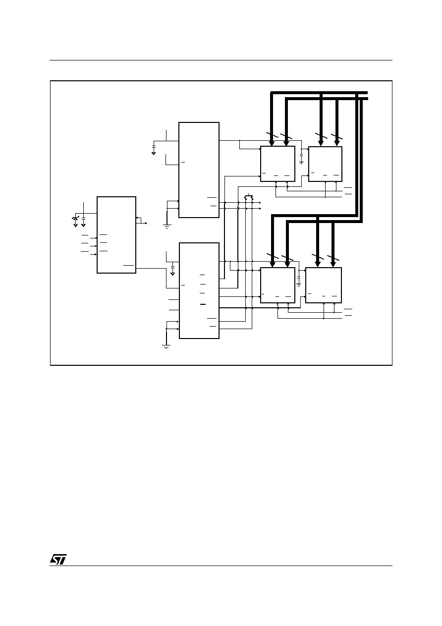
Figure 3. Logic Diagram
Table 1. Signal Names
AI04217
VCC
M48T254V
VSS
BL
A0 ≠ A20
DQ0 ≠ DQ7
WE
OE
CE
A0 - A20
Address Inputs
DQ0 - DQ7
Data Input/Output
CE
Chip Enable
WE
WRITE Enable Inputs
OE
Output Enable
BL
Battery Low Output (Open Drain)
NC
No Connect
V
CC
Supply Voltage
V
SS
Ground