1/27
March 2003
Rev. 4.0
M48T37Y
M48T37V
5.0 or 3.3V, 256 Kbit (32 Kbit x 8) TIMEKEEPER
Æ
SRAM
FEATURES SUMMARY
s
INTEGRATED ULTRA-LOW POWER SRAM,
REAL TIME CLOCK, POWER-FAIL CONTROL
CIRCUIT, and BATTERY
s
FREQUENCY TEST OUTPUT FOR REAL
TIME CLOCK SOFTWARE CALIBRATION
s
YEAR 2000 COMPLIANT
s
AUTOMATIC POWER-FAIL CHIP DESELECT
and WRITE PROTECTION
s
WATCHDOG TIMER
s
WRITE PROTECT VOLTAGE
(V
PFD
= Power-Fail Deselect Voltage):
≠ M48T37Y: V
CC
= 4.5 to 5.5V
4.2V
V
PFD
4.5V
≠ M48T37V: V
CC
= 3.0 to 3.6V
2.7V
V
PFD
3.0V
s
PACKAGING INCLUDES A 44-LEAD SOIC and
SNAPHAT
Æ
TOP (to be Ordered Separately)
s
SOIC PACKAGE PROVIDES DIRECT
CONNECTION FOR A SNAPHAT TOP WHICH
CONTAINS THE BATTERY and CRYSTAL
s
MICROPROCESSOR POWER-ON RESET
(Valid even during battery back-up mode)
s
PROGRAMMABLE ALARM OUTPUT ACTIVE
IN THE BATTERY BACK-UP MODE
s
BATTERY LOW FLAG
Figure 1. 44-pin SOIC Package
44
1
SNAPHAT (SH)
Battery/Crystal
SOH44 (MH)

M48T37Y, M48T37V
2/27
TABLE OF CONTENTS
SUMMARY DESCRIPTION . . . . . . . . . . . . . . . . . . . . . . . . . . . . . . . . . . . . . . . . . . . . . . . . . . . . . . . . . . . 4
Figure 2. Logic Diagram . . . . . . . . . . . . . . . . . . . . . . . . . . . . . . . . . . . . . . . . . . . . . . . . . . . . . . . . . . 4
Table 1. Signal Names . . . . . . . . . . . . . . . . . . . . . . . . . . . . . . . . . . . . . . . . . . . . . . . . . . . . . . . . . . . 4
Figure 3. SOIC Connections . . . . . . . . . . . . . . . . . . . . . . . . . . . . . . . . . . . . . . . . . . . . . . . . . . . . . . . 4
Figure 4. Block Diagram . . . . . . . . . . . . . . . . . . . . . . . . . . . . . . . . . . . . . . . . . . . . . . . . . . . . . . . . . . 5
MAXIMUM RATING. . . . . . . . . . . . . . . . . . . . . . . . . . . . . . . . . . . . . . . . . . . . . . . . . . . . . . . . . . . . . . . . . 6
Table 2. Absolute Maximum Ratings . . . . . . . . . . . . . . . . . . . . . . . . . . . . . . . . . . . . . . . . . . . . . . . . . 6
DC AND AC PARAMETERS. . . . . . . . . . . . . . . . . . . . . . . . . . . . . . . . . . . . . . . . . . . . . . . . . . . . . . . . . . 7
Table 3. Operating and AC Measurement Conditions . . . . . . . . . . . . . . . . . . . . . . . . . . . . . . . . . . . . 7
Figure 5. AC Testing Load Circuit . . . . . . . . . . . . . . . . . . . . . . . . . . . . . . . . . . . . . . . . . . . . . . . . . . . 7
Table 4. Capacitance. . . . . . . . . . . . . . . . . . . . . . . . . . . . . . . . . . . . . . . . . . . . . . . . . . . . . . . . . . . . . 7
Table 5. DC Characteristics. . . . . . . . . . . . . . . . . . . . . . . . . . . . . . . . . . . . . . . . . . . . . . . . . . . . . . . . 8
OPERATION MODES . . . . . . . . . . . . . . . . . . . . . . . . . . . . . . . . . . . . . . . . . . . . . . . . . . . . . . . . . . . . . . . 9
Table 6. Operating Modes . . . . . . . . . . . . . . . . . . . . . . . . . . . . . . . . . . . . . . . . . . . . . . . . . . . . . . . . . 9
READ Mode . . . . . . . . . . . . . . . . . . . . . . . . . . . . . . . . . . . . . . . . . . . . . . . . . . . . . . . . . . . . . . . . . . 10
Figure 6. READ Mode AC Waveforms . . . . . . . . . . . . . . . . . . . . . . . . . . . . . . . . . . . . . . . . . . . . . . 10
Table 7. READ Mode AC Characteristics . . . . . . . . . . . . . . . . . . . . . . . . . . . . . . . . . . . . . . . . . . . . 10
WRITE Mode. . . . . . . . . . . . . . . . . . . . . . . . . . . . . . . . . . . . . . . . . . . . . . . . . . . . . . . . . . . . . . . . . . 11
Figure 7. WRITE Enable Controlled, WRITE AC Waveform . . . . . . . . . . . . . . . . . . . . . . . . . . . . . . 11
Figure 8. Chip Enable Controlled, WRITE AC Waveforms . . . . . . . . . . . . . . . . . . . . . . . . . . . . . . . 11
WRITE Mode AC Characteristics . . . . . . . . . . . . . . . . . . . . . . . . . . . . . . . . . . . . . . . . . . . . . . . . . 12
Data Retention Mode . . . . . . . . . . . . . . . . . . . . . . . . . . . . . . . . . . . . . . . . . . . . . . . . . . . . . . . . . . . 13
Figure 9. Power Down/Up Mode AC Waveforms . . . . . . . . . . . . . . . . . . . . . . . . . . . . . . . . . . . . . . 13
Table 9. Power Down/Up AC Characteristics . . . . . . . . . . . . . . . . . . . . . . . . . . . . . . . . . . . . . . . . . 13
Table 10. Power Down/Up Trip Points DC Characteristics . . . . . . . . . . . . . . . . . . . . . . . . . . . . . . . 14
CLOCK OPERATIONS . . . . . . . . . . . . . . . . . . . . . . . . . . . . . . . . . . . . . . . . . . . . . . . . . . . . . . . . . . . . . 14
Reading the Clock . . . . . . . . . . . . . . . . . . . . . . . . . . . . . . . . . . . . . . . . . . . . . . . . . . . . . . . . . . . . . 14
Setting the Clock . . . . . . . . . . . . . . . . . . . . . . . . . . . . . . . . . . . . . . . . . . . . . . . . . . . . . . . . . . . . . . 14
Stopping and Starting the Oscillator . . . . . . . . . . . . . . . . . . . . . . . . . . . . . . . . . . . . . . . . . . . . . . 14
Table 11. Register Map . . . . . . . . . . . . . . . . . . . . . . . . . . . . . . . . . . . . . . . . . . . . . . . . . . . . . . . . . . 15
Setting the Alarm Clock . . . . . . . . . . . . . . . . . . . . . . . . . . . . . . . . . . . . . . . . . . . . . . . . . . . . . . . . 16
Figure 10. Alarm Interrupt Reset Waveform . . . . . . . . . . . . . . . . . . . . . . . . . . . . . . . . . . . . . . . . . . 16
Table 12. Alarm Repeat Modes . . . . . . . . . . . . . . . . . . . . . . . . . . . . . . . . . . . . . . . . . . . . . . . . . . . . 16
Figure 11. Back-up Mode Alarm Waveforms. . . . . . . . . . . . . . . . . . . . . . . . . . . . . . . . . . . . . . . . . . 17
Calibrating the Clock. . . . . . . . . . . . . . . . . . . . . . . . . . . . . . . . . . . . . . . . . . . . . . . . . . . . . . . . . . . 17

3/27
M48T37Y, M48T37V
Watchdog Timer . . . . . . . . . . . . . . . . . . . . . . . . . . . . . . . . . . . . . . . . . . . . . . . . . . . . . . . . . . . . . . 18
Power-on Reset . . . . . . . . . . . . . . . . . . . . . . . . . . . . . . . . . . . . . . . . . . . . . . . . . . . . . . . . . . . . . . . 18
Programmable Interrupts . . . . . . . . . . . . . . . . . . . . . . . . . . . . . . . . . . . . . . . . . . . . . . . . . . . . . . . 19
Battery Low Flag . . . . . . . . . . . . . . . . . . . . . . . . . . . . . . . . . . . . . . . . . . . . . . . . . . . . . . . . . . . . . . 19
Initial Power-on Defaults. . . . . . . . . . . . . . . . . . . . . . . . . . . . . . . . . . . . . . . . . . . . . . . . . . . . . . . . 19
Table 13. Default Values . . . . . . . . . . . . . . . . . . . . . . . . . . . . . . . . . . . . . . . . . . . . . . . . . . . . . . . . . 19
Figure 12. Crystal Accuracy Across Temperature . . . . . . . . . . . . . . . . . . . . . . . . . . . . . . . . . . . . . . 20
Figure 13. Clock Calibration . . . . . . . . . . . . . . . . . . . . . . . . . . . . . . . . . . . . . . . . . . . . . . . . . . . . . . 20
V
CC
Noise And Negative Going Transients. . . . . . . . . . . . . . . . . . . . . . . . . . . . . . . . . . . . . . . . . 21
Figure 14. Supply Voltage Protection . . . . . . . . . . . . . . . . . . . . . . . . . . . . . . . . . . . . . . . . . . . . . . . 21
PACKAGE MECHANICAL INFORMATION . . . . . . . . . . . . . . . . . . . . . . . . . . . . . . . . . . . . . . . . . . . . . 22
PART NUMBERING . . . . . . . . . . . . . . . . . . . . . . . . . . . . . . . . . . . . . . . . . . . . . . . . . . . . . . . . . . . . . . . 25
Table 18. SNAPHAT Battery Table . . . . . . . . . . . . . . . . . . . . . . . . . . . . . . . . . . . . . . . . . . . . . . . . . 25
REVISION HISTORY. . . . . . . . . . . . . . . . . . . . . . . . . . . . . . . . . . . . . . . . . . . . . . . . . . . . . . . . . . . . . . . 26
M48T37Y, M48T37V
4/27
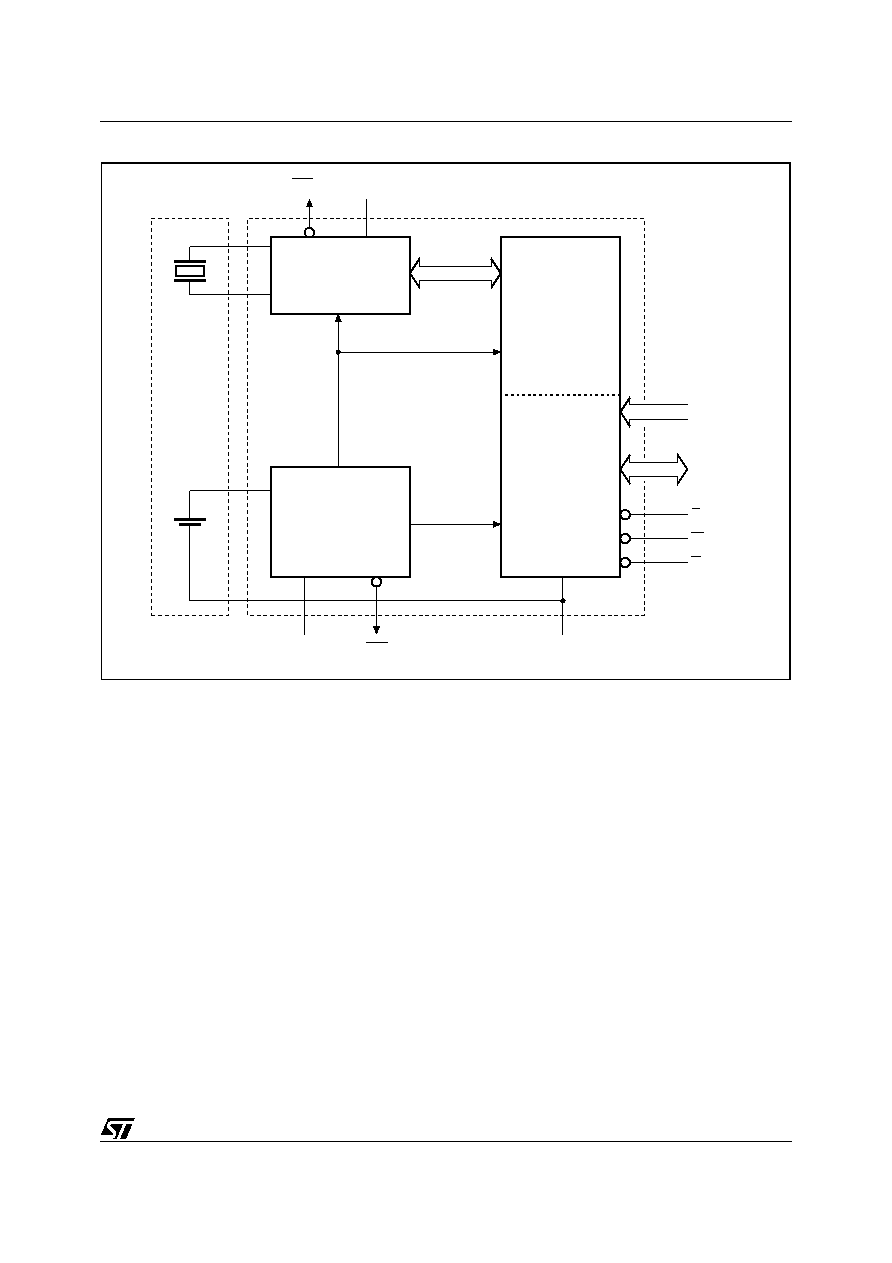
SUMMARY DESCRIPTION
The M48T37Y/V TIMEKEEPER
Æ
RAM is a 32 Kb
x8 non-volatile static RAM and real time clock. The
monolithic chip is available in a special package
which provides a highly integrated battery backed-
up memory and real time clock solution.
The 44-lead, 330mil SOIC package provides sock-
ets with gold-plated contacts at both ends for di-
rect connection to a separate SNAPHAT housing
containing the battery and crystal. The unique de-
sign allows the SNAPHAT
Æ
battery/crystal pack-
age to be mounted on top of the SOIC package
after the completion of the surface mount process.
Insertion of the SNAPHAT housing after reflow
prevents potential battery and crystal damage due
to the high temperatures required for device sur-
face-mounting. The SNAPHAT housing is keyed
to prevent reverse insertion.
The SOIC and battery packages are shipped sep-
arately in plastic anti-static tubes or in Tape &Reel
form. For the 44-lead SOIC, the battery/crystal
package (e.g., SNAPHAT) part number is "M4T28-
BR12SH" or "M4T32-BR12SH" (see Table 18,
page 25).
Caution: Do not place the SNAPHAT battery/crys-
tal top in conductive foam, as this will drain the lith-
ium button-cell battery.
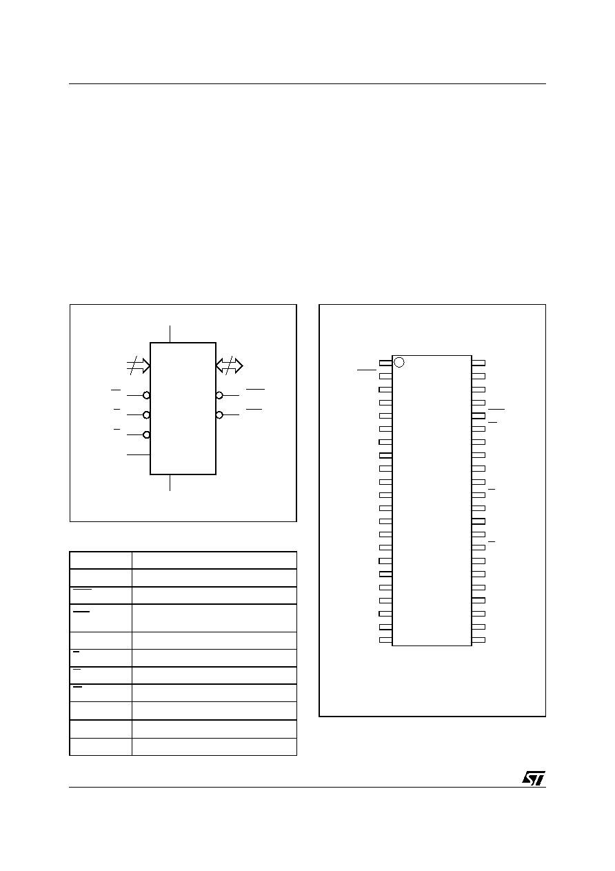
Figure 2. Logic Diagram
Table 1. Signal Names
Figure 3. SOIC Connections
A0-A14
Address Inputs
DQ0-DQ7
Data Inputs / Outputs
RST
Reset Output (Open Drain)
IRQ/FT
Interrupt / Frequency Test Output
(Open Drain)
WDI
Watchdog Input
E
Chip Enable
G
Output Enable
W
WRITE Enable
V
CC
Supply Voltage
V
SS
Ground
NC
Not connected Internally
AI02172
8
DQ0-DQ7
W
VCC
M48T37Y
M48T37V
VSS
G
E
WDI
RST
IRQ/FT
15
A0-A14
AI02174
22
44
43
VSS
1
A1
A7
A4
A3
A2
A6
A5
A13
NC
A8
A9
NC
A11
G
E
VCC
M48T37Y
M48T37V
10
2
5
6
7
8
9
11
12
13
14
15
21
40
39
36
35
34
33
32
31
30
29
28
A12
A14
IRQ/FT
NC
3
4
38
37
42
41
A0
DQ0
DQ7
DQ5
DQ1
DQ2
DQ3
DQ4
DQ6
16
17
18
19
20
27
26
25
24
23
WDI
NC
NC
RST
NC
NC
NC
A10
NC
NC
W
NC
NC
NC