1/20
February 2000
M48T37Y
M48T37V
3.3V-5V 256 Kbit (32Kb x8) TIMEKEEPER
Æ
SRAM
s
INTEGRATED ULTRA-LOW POWER SRAM,
REAL TIME CLOCK, POWER-FAIL CONTROL
CIRCUIT and BATTERY
s
FREQUENCY TEST OUTPUT for REAL TIME
CLOCK SOFTWARE CALIBRATION
s
YEAR 2000 COMPLIANT
s
AUTOMATIC POWER-FAIL CHIP DESELECT
and WRITE PROTECTION
s
WATCHDOG TIMER
s
WRITE PROTECT VOLTAGE
(V
PFD
= Power-Fail Deselect Voltage):
≠ M48T37Y: 4.2V
V
PFD
4.5V
≠ M48T37V: 2.7V
V
PFD
3.0V
s
PACKAGING INCLUDES a 44-LEAD SOIC and
SNAPHAT TOP (to be Ordered Separately)
s
SOIC PACKAGE PROVIDES DIRECT
CONNECTION for a SNAPHAT
Æ
TOP which
CONTAINS the BATTERY and CRYSTAL
s
MICROPROCESSOR POWER-ON RESET
(Valid even during battery back-up mode)
s
PROGRAMMABLE ALARM OUTPUT ACTIVE
in the BATTERY BACKED-UP
s
BATTERY LOW FLAG
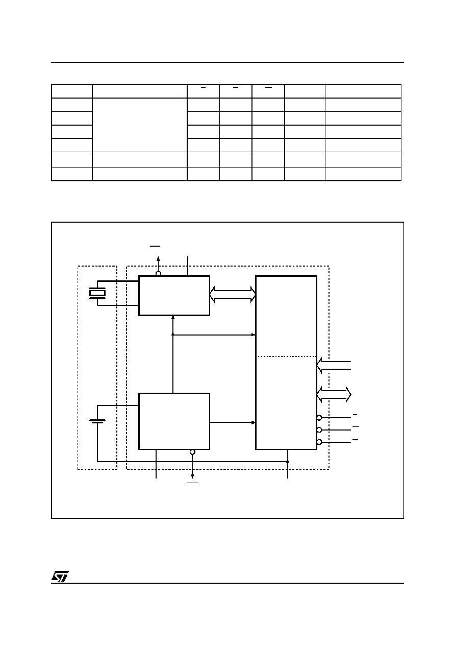
Figure 1. Logic Diagram
AI02172
8
DQ0-DQ7
W
VCC
M48T37Y
M48T37V
VSS
G
E
WDI
RST
IRQ/FT
15
A0-A14
Table 1. Signal Names
A0-A14
Address Inputs
DQ0-DQ7
Data Inputs / Outputs
RST
Power Fail Reset Output (Open Drain)
IRQ/FT
Interrupt / Frequency Test Output
(Open Drain)
WDI
Watchdog Input
E
Chip Enable
G
Output Enable
W
Write Enable
V
CC
Supply Voltage
V
SS
Ground
NC
Not connected Internally
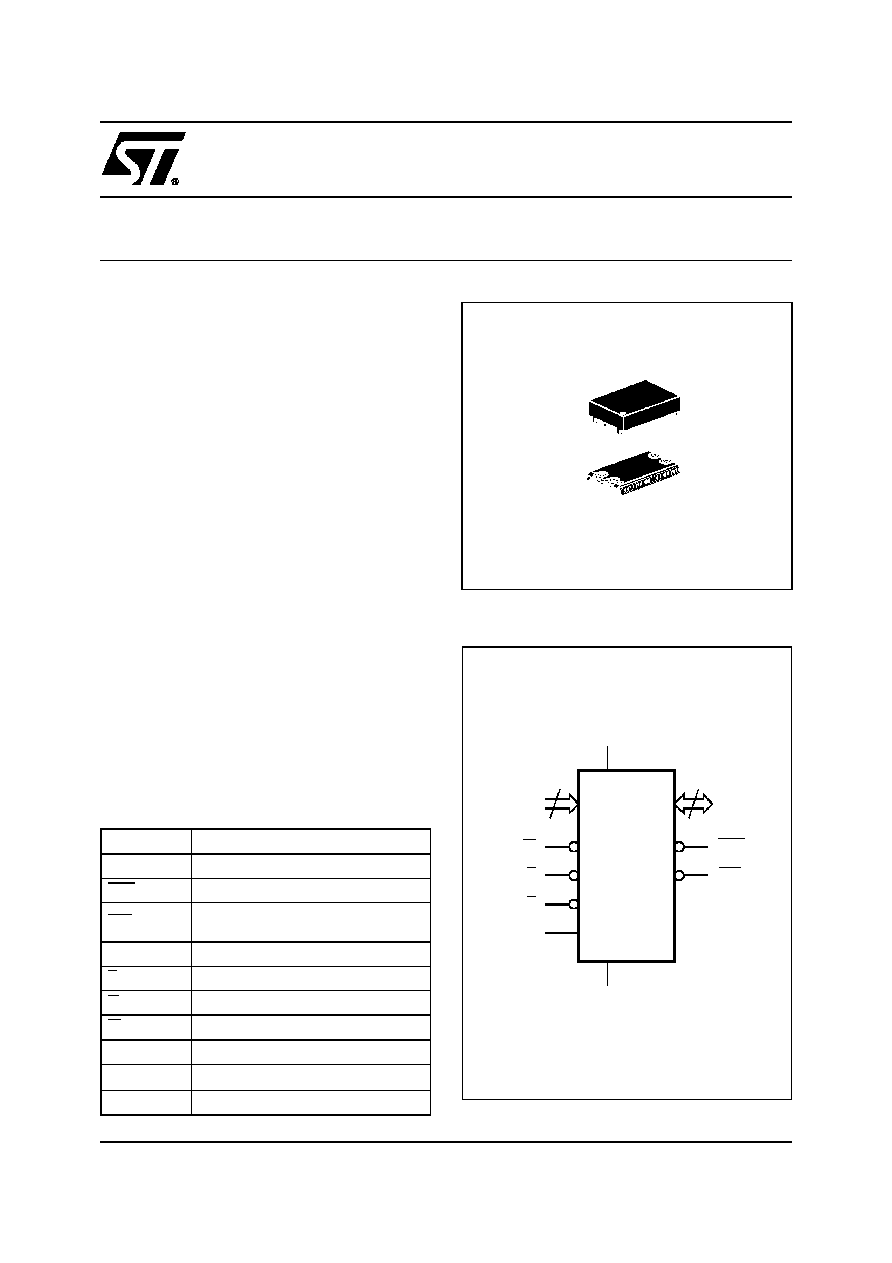
SOH44 (MH)
SNAPHAT (SH)
Battery
44
1
M48T37Y, M48T37V
2/20
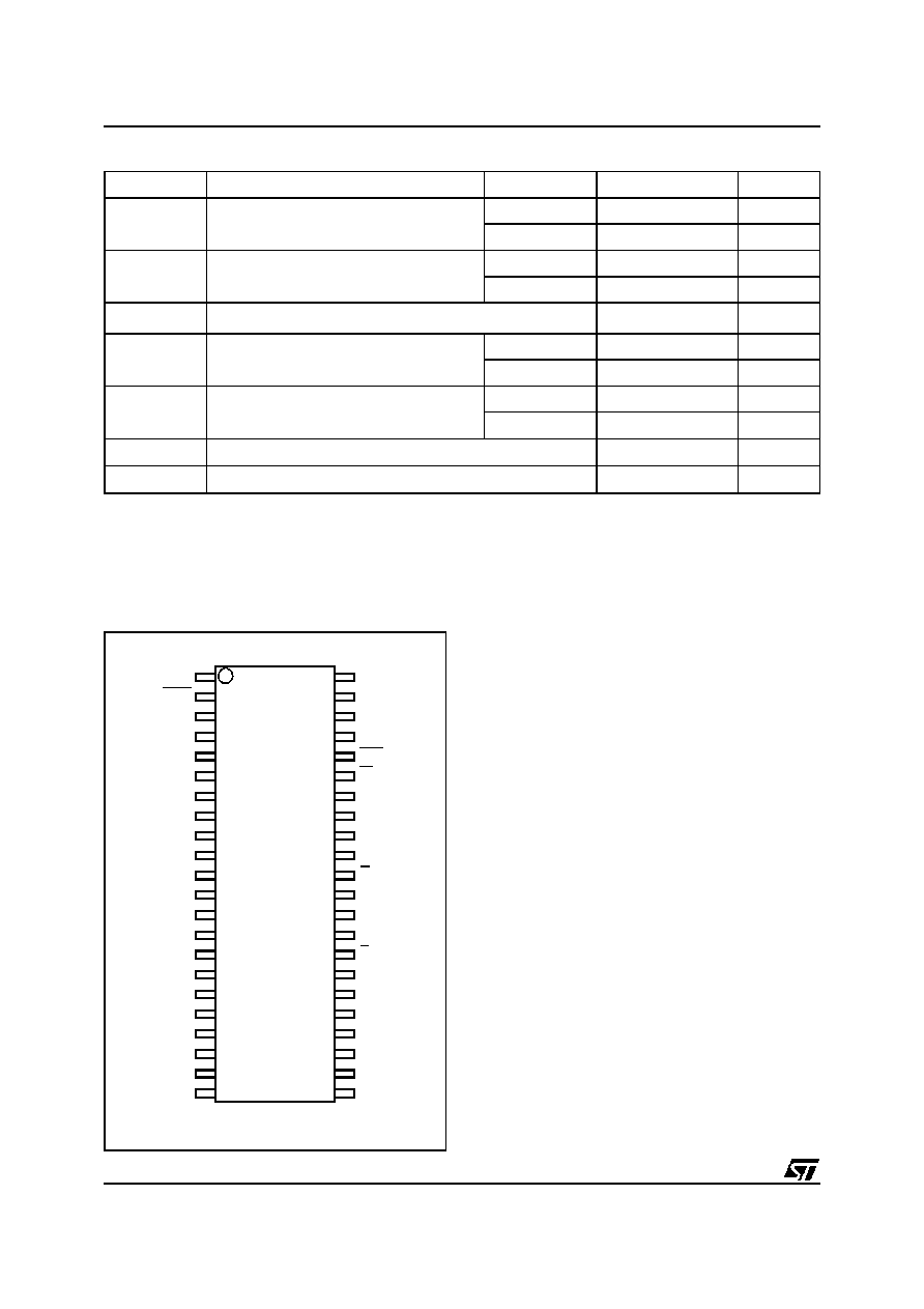
Figure 2. SOIC Connections
AI02174
22
44
43
VSS
1
A1
A7
A4
A3
A2
A6
A5
A13
NC
A8
A9
NC
A11
G
E
VCC
M48T37Y
M48T37V
10
2
5
6
7
8
9
11
12
13
14
15
21
40
39
36
35
34
33
32
31
30
29
28
A12
A14
IRQ/FT
NC
3
4
38
37
42
41
A0
DQ0
DQ7
DQ5
DQ1
DQ2
DQ3
DQ4
DQ6
16
17
18
19
20
27
26
25
24
23
WDI
NC
NC
RST
NC
NC
NC
A10
NC
NC
W
NC
NC
NC
Table 2. Absolute Maximum Ratings
(1)
Note: 1. Stresses greater than those listed under "Absolute Maximum Ratings" may cause permanent damage to the device. This is a stress
rating only and functional operation of the device at these or any other conditions above those indicated in the operational section
of this specification is not implied. Exposure to the absolute maximum rating conditions for extended periods of time may affect
reliability.
2. Soldering temperature not to exceed 260
∞
C for 10 seconds (total thermal budget not to exceed 150
∞
C for longer than 30 seconds).
CAUTION: Negative undershoots below ≠0.3V are not allowed on any pin while in the Battery Back-up mode.
CAUTION: Do NOT wave solder SOIC to avoid damaging SNAPH AT sockets.
Symbol
Parameter
Value
Unit
T
A
Ambient Operating Temperature
Grade 1
0 to 70
∞
C
Grade 6
≠40 to 85
∞
C
T
STG
Storage Temperature (V
CC
Off, Oscillator Off)
SNAPHAT
≠40 to 85
∞
C
SOIC
≠55 to 125
∞
C
T
SLD
(2)
Lead Solder Temperature for 10 seconds
260
∞
C
V
IO
Input or Output Voltages
M48T37Y
≠0.3 to 7
V
M48T37V
≠0.3 to 4.6
V
V
CC
Supply Voltage
M48T37Y
≠0.3 to 7
V
M48T37V
≠0.3 to 4.6
V
I
O
Output Current
10
mA
P
D
Power Dissipation
1
W
DESCRIPTION
The M48T37Y/37V TIMEKEEPER
Æ
RAM is a
32Kb x8 non-volatile static RAM and real time
clock. The monolithic chip is available in a special
package which provides a highly integrated bat-
tery backed-up memory and real time clock solu-
tion.
The 44 lead 330mil SOIC package provides sock-
ets with gold-plated contacts at both ends for di-
rect connection to a separate SNAPHAT housing
containing the battery and crystal. The unique de-
sign allows the SNAPHAT battery package to be
mounted on top of the SOIC package after the
completion of the surface mount process.
Insertion of the SNAPHAT housing after reflow
prevents potential battery and crystal damage due
to the high temperatures required for device sur-
face-mounting. The SNAPHAT housing is keyed
to prevent reverse insertion.
The SOIC and battery packages are shipped sep-
arately in plastic anti-static tubes or in Tape &Reel
form. For the 44 lead SOIC, the battery/crystal
package (i.e. SNAPHAT) part number is "M4T28-
BR12SH" or "M4T32-BR12SH".
Caution: Do not place the SNAPHAT battery/crys-
tal top in conductive foam, as this will drain the lith-
ium button-cell battery.
As Figure 3 shows, the static memory array and
the quartz controlled clock oscillator of the
M48T37Y/37V are integrated on one silicon chip.
M48T37Y, M48T37V
4/20
The memory locations, to provide user accessible
BYTEWIDE
TM
clock information are in the bytes
with addresses 7FF1 and 7FF9h-7FFFh (located
in Table 11). The clock locations contain the cen-
tury, year, month, date, day, hour, minute, and
second in 24 hour BCD format. Corrections for 28,
29 (leap year-compliant until the year 2100), 30,
and 31 day months are made automatically.
Byte 7FF8h is the clock control register. This byte
controls user access to the clock information and
also stores the clock calibration setting.
Byte 7FF7h contains the watchdog timer setting.
The watchdog timer redirects an out-of-control mi-
croprocessor and provides a reset or interrupt to it.
Byte 7FF2h-7FF5h are reserved for clock alarm
programming.
These bytes can be used to set the alarm. This will
generate an active low signal on the IRQ/FT pin
when the alarm bytes match the date, hours, min-
utes and seconds of the clock. The eight clock
bytes are not the actual clock counters them-
selves; they are memory locations consisting of Bi-
PORT
TM
read/write memory cells. The M48T37Y/
37V includes a clock control circuit which updates
the clock bytes with current information once per
second. The information can be accessed by the
user in the same manner as any other location in
the static memory array.
The M48T37Y/37V also has its own Power-fail De-
tect circuit. The control circuitry constantly moni-
tors the single V
CC
supply for an out of tolerance
condition. When V
CC
is out of tolerance, the circuit
writes protects the SRAM, providing a high degree
of data security in the midst of unpredictable sys-
tem operation brought on by low V
CC
. As V
CC
falls
below the Battery Back-up Switchover Voltage
(V
SO
), the control circuitry connects the battery
which maintains data and clock operation until val-
id power returns.
READ MODE
The M48T37Y/37V is in the Read Mode whenever
Write Enable (W) is high and Chip Enable (E) is
low. The unique address specified by the 15 Ad-
dress Inputs defines which one of the 32,752 bytes
of data is to be accessed. Valid data will be avail-
able at the Data I/O pins within Address Access
time (t
AVQV
) after the last address input signal is
stable, providing that the E and Output Enable (G)
access times are also satisfied. If the E and G ac-
cess times are not met, valid data will be available
after the latter of the Chip Enable Access time
(t
ELQV
) or Output Enable Access time (t
GLQV
).
The state of the eight three-state Data I/O signals
is controlled by E and G. If the outputs are activat-
ed before t
AVQV
, the data lines will be driven to an
indeterminate state until t
AVQV
.
If the Address Inputs are changed while E and G
remain active, output data will remain valid for Out-
put Data Hold time (t
AXQX
) but will be indetermi-
nate until the next Address Access.
Table 4. AC Measurement Conditions
Note that Output Hi-Z is defined as the point where data is no longer
driven.
Input Rise and Fall Times
5ns
Input Pulse Voltages
0 to 3V
Input and Output Timing Ref. Voltages
1.5V
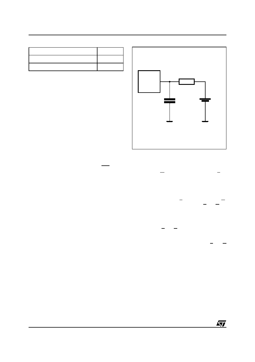
Figure 4. AC Testing Load Circuit
Note: Excluding open-drain output pins.
AI02325
CL = 100pF
CL includes JIG capacitance
645
DEVICE
UNDER
TEST
1.75V
5/20
M48T37Y, M48T37V
Table 6. DC Characteristics
(T
A
= 0 to 70
∞
C or ≠40 to 85
∞
C)
Note: 1. Outputs deselected.
2. Negative spikes of ≠1V allowed for up to 10ns once per cycle.
Symbol
Parameter
Test Condition
M48T37Y
M48T37V
Unit
V
CC
= 4.5V to 5.5V
V
CC
= 3.0V to 3.6V
Min
Max
Min
Max
I
LI
(1)
Input Leakage Current
0V
V
IN
V
CC
±
1
±
1
µ
A
I
LO
(1)
Output Leakage Current
0V
V
OUT
V
CC
±
1
±
1
µ
A
I
CC
Supply Current
Outputs open
50
33
mA
I
CC1
Supply Current (Standby)
TTL
E = V
IH
3
2
mA
I
CC2
Supply Current (Standby)
CMOS
E = V
CC
≠ 0.2V
3
2
mA
V
IL
(2)
Input Low Voltage
≠0.3
0.8
≠0.3
0.8
V
V
IH
Input High Voltage
2.2
V
CC
+ 0.3
2.2
V
CC
+ 0.3
V
V
OL
Output Low Voltage
(standard)
I
OL
= 2.1mA
0.4
0.4
V
V
OL
Output Low Voltage
(open drain)
I
OL
= 10mA
0.4
0.4
V
V
OH
(2)
Output High Voltage
I
OH
= ≠1mA
2.4
2.4
V
Table 5. Capacitance
(1, 2)
(T
A
= 25
∞
C)
Note: 1. Effective capacitance measured with power supply at 5V.
2. Sampled only, not 100% tested.
3. Outputs deselected.
Symbol
Parameter
Test Condit ion
Min
Max
Unit
C
IN
Input Capacitance
V
IN
= 0V
10
pF
C
IO
(3)
Input / Output Capacitance
V
OUT
= 0V
10
pF