 | –≠–ª–µ–∫—Ç—Ä–æ–Ω–Ω—ã–π –∫–æ–º–ø–æ–Ω–µ–Ω—Ç: P0102BL | –°–∫–∞—á–∞—Ç—å:  PDF PDF  ZIP ZIP |
1/5
Æ
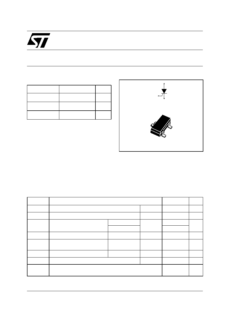
P0102BL
SENSITIVE
0.25A SCRs
September 2000 - Ed: 3
MAIN FEATURES:
DESCRIPTION
Thanks to highly sensitive triggering levels, the
PO102BL SCR is suitable for all applications
where the available gate current is limited such as
stand-by mode power supplies, smoke and alarm
detectors...
Available in SOT-23, it provides optimized space
saving on high density printed circuit boards.
Symbol Value
Unit
I
T(RMS)
0.25
A
V
DRM
/V
RRM
200
V
I
GT
200
µA
ABSOLUTE RATINGS (limiting values)
Symbol
Parameter Value
Unit
I
T(RMS)
RMS on-state current (180∞ conduction angle)
Tamb = 30∞C
0.25
A
I
T(AV)
Average on-state current (180∞ conduction angle)
Tamb = 30∞C
0.17
A
I
TSM
Non repetitive surge peak on-state
current
tp = 8.3 ms
Tj = 25∞C
7
A
tp = 10 ms
6
I
≤
t
I
≤
t Value for fusing
tp = 10 ms
Tj = 25∞C
0.18
A
2
S
dI/dt
Critical rate of rise of on-state current
I
G
= 2 x I
GT
, tr
100ns
F = 60 Hz
Tj = 125∞C
50
A/µs
I
GM
Peak gate current
tp = 20 µs
Tj = 125∞C
0.5
A
P
G(AV)
Average gate power dissipation
Tj = 125∞C
0.02
W
T
stg
Tj
Storage junction temperature range
Operating junction temperature range
- 40 to + 150
- 40 to + 125
∞C
G
A
K
A
G
K
SOT-23
P0102BL
2/5
ELECTRICAL CHARACTERISTICS (Tj = 25∞C, unless otherwise specified)
THERMAL RESISTANCES
PRODUCT SELECTOR
ORDERING INFORMATION
OTHER INFORMATION
Symbol
Test Conditions
P0102BL
Unit
I
GT
V
D
= 12 V R
L
= 140
MAX.
200
µA
V
GT
MAX.
0.8
V
V
GD
V
D
= V
DRM
R
L
= 3.3 k
R
GK
= 1 k
Tj = 125∞C
MIN.
0.1
V
V
RG
I
RG
= 10 µA
MIN.
8
V
I
H
I
T
= 50 mA R
GK
= 1k
MAX.
6
mA
I
L
I
G
= 1 mA R
GK
= 1k
MAX.
7
mA
dV/dt
V
D
= 67 % V
DRM
R
GK
= 1k
Tj = 125∞C
MIN.
200
V/µs
V
TM
I
TM
= 0.4 A
tp = 380 µs
Tj = 25∞C
MAX.
1.7
V
V
t0
Threshold voltage
Tj = 125∞C
MAX.
1.0
V
R
d
Dynamic resistance
Tj = 125∞C
MAX.
1000
m
I
DRM
I
RRM
V
DRM
= V
RRM
Tj = 25∞C
MAX.
1
µA
Tj = 125∞C
100
Symbol
Parameter
Value
Unit
R
th(j-a)
Junction to ambient (mounted on FR4 with recommended pad layout)
400
∞C/W
Part Number
Voltage
Sensitivity
Package
P0102BL
200 V
200 µA
SOT-23
Part Number
Marking
Weight
Base quantity
Packing mode
P0102BL
P2B
0.01 g
3000
Tape & reel
P 01 02 B L 5AA4
Blank
SENSITIVE
SCR
SERIES
CURRENT: 0.25A
SENSITIVITY:
02: 200µA
VOLTAGE:
B: 200V
PACKAGE:
L: SOT-23
PACKING MODE:
Tape & Reel
P0102BL
3/5
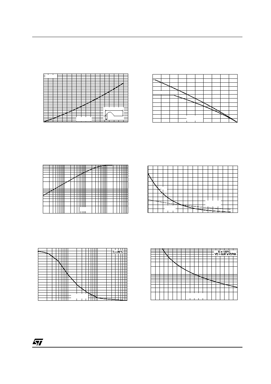
Fig. 1: Maximum average power dissipation
versus average on-state current.
Fig. 2: Average and D.C. on-state current versus
ambient temperature.
Fig. 3: Relative variation of thermal impedance
junction to ambient versus pulse duration.
Fig. 4: Relative variation of gate trigger current,
holding current and latching current versus
junction temperature (typical values).
Fig. 5: Relative variation of holding current
versus gate-cathode resistance (typical values).
Fig. 6: Relative variation of dV/dt immunity
versus gate-cathode resistance (typical values).
0.00 0.02 0.04 0.06 0.08 0.10 0.12 0.14 0.16 0.18
0.00
0.02
0.04
0.06
0.08
0.10
0.12
0.14
0.16
0.18
0.20
0.22
0.24
0.26
0.28
0.30
P(W)
360 ∞
= 180 ∞
IT(av)(A)
0
25
50
75
100
125
0.00
0.05
0.10
0.15
0.20
0.25
0.30
IT(av)(A)
= 180∞
D.C
Tamb(∞C)
1E-2
1E-1
1E+0
1E+1
1E+2
0.01
0.10
1.00
K=[Zth(j-a)/Rth(j-a)]
tp(s)
-40
-20
0
20
40
60
80
100
120
140
0
1
2
3
4
5
6
IGT, IH, IL[Tj] / IGT , IH, IL[Tj = 25 ∞C]
IH & IL
(Rgk = 1k
)
IGT
Tj(∞C)
IH[Rgk] / IH[Rgk = 1k ]
Rgk(k
)
20
18
16
14
12
10
8
6
4
2
0
1E-2
1E-1
1E+0
1E+1
dV/dt[Rgk] / dV/dt[Rgk = 1k ]
Rgk(k
)
10.0
1.0
0.1
0
0.2
0.4
0.6
0.8
1.0
1.2
1.4
1.6
1.8
2.0

P0102BL
4/5
Fig. 7: Relative variation of dV/dt immunity
versus gate-cathode capacitance (typical values).
Fig. 8: Surge peak on-state current versus
number of cycles.
Fig. 9: Non-repetitive surge peak on-state
current for a sinusoidal pulse with width
tp < 10ms, and corresponding value of I≤t.
Fig. 10: On-state characteristics (maximum
values).
Fig. 11: Thermal resistance junction to ambient
versus copper surface under tab (Epoxy printed
circuit board FR4, copper thickness: 35
µ
m).
0
1
2
3
4
5
6
7
0
2
4
6
8
10
VD = 0.67 x VDRM
Tj = 125 ∞C
Rgk = 1k
dV/dt[Cgk] / dV/dt [Rgk = 1k
]
Cgk(nF)
ITSM(A)
Number of cycles
1
0
1
2
3
4
5
6
7
10
100
1000
0.01
0.10
1.00
10.00
0.1
1.0
10.0
100.0
ITSM(A),I
2
t(A
2
s)
Tj initial = 25 ∞C
ITSM
I
2
t
tp(ms)
0.5 1.0 1.5 2.0 2.5 3.0 3.5 4.0 4.5 5.0 5.5 6.0
1E-2
1E-1
1E+0
1E+1
ITM(A)
Tj max.:
Vto = 1.00 V
Rd = 1
Tj = Tj max.
Tj = 25∞C
VTM(V)
0
10
20
30
40
50
60
70
80
90
100
0
100
200
300
400
500
Rth(j-a) (∞C/W)
S (mm
2
)
P0102BL
5/5
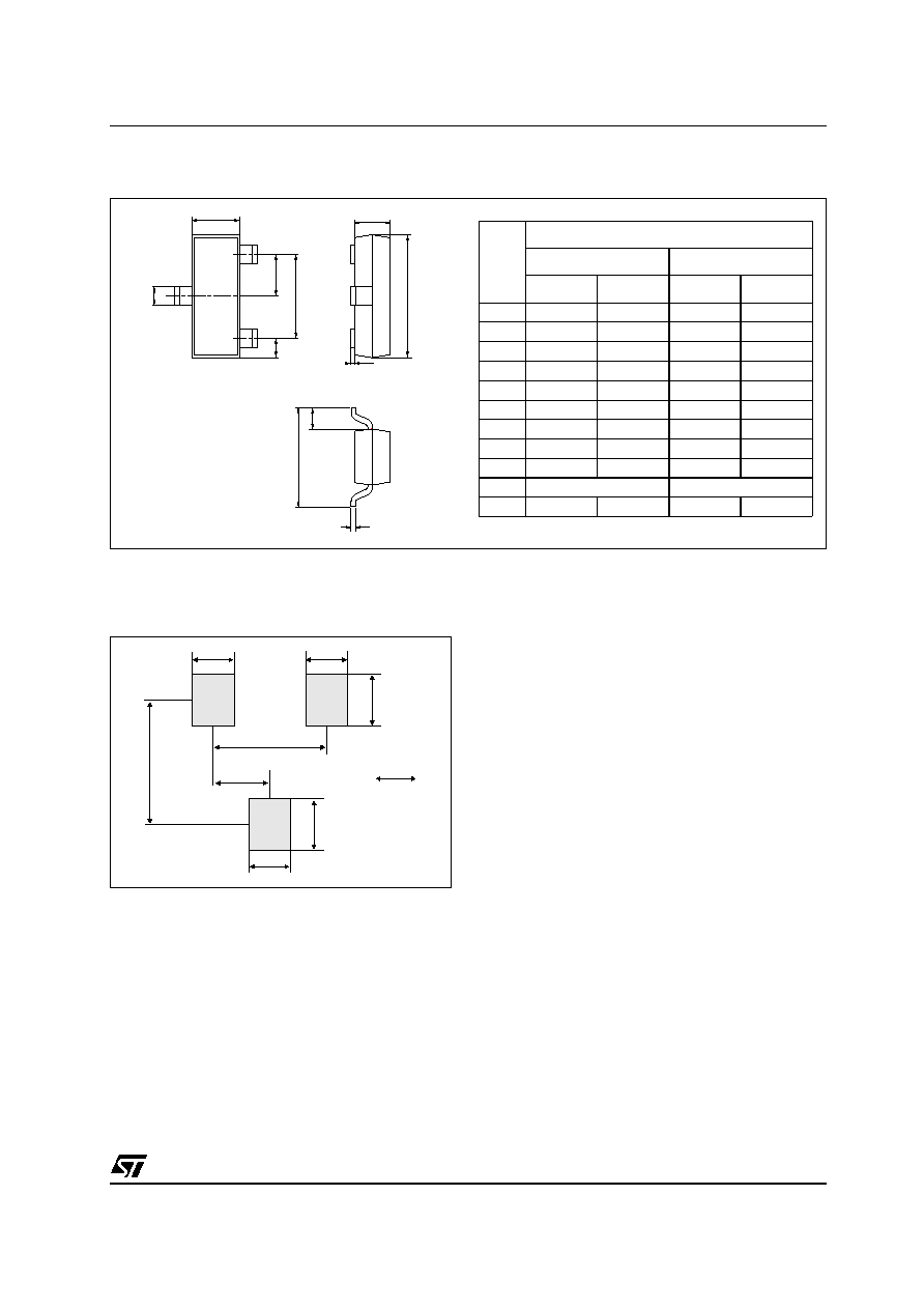
PACKAGE MECHANICAL DATA
SOT-23 (Plastic)
REF.
DIMENSIONS
Millimeters
Inches
Min.
Max.
Min.
Max.
A
0.89
1.4
0.035
0.055
A1
0
0.1
0
0.004
B
0.3
0.51
0.012
0.02
c
0.085
0.18
0.003
0.007
D
2.75
3.04
0.108
0.12
e
0.85
1.05
0.033
0.041
e1
1.7
2.1
0.067
0.083
E
1.2
1.6
0.047
0.063
H
2.1
2.75
0.083
0.108
L
0.6 typ.
0.024 typ.
S
0.35
0.65
0.014
0.026
B
E
S
e
e1
A
D
c
L
H
A1
FOOTPRINT DIMENSIONS (in millimeters)
SOT-23 (Plastic)
0.9
0.035
0.9
0.035
1.9
0.075
mm
inch
2.35
0.92
1.1
0.043
1.1
0.043
1.45
0.037
0.9
0.035
Information furnished is believed to be accurate and reliable. However, STMicroelectronics assumes no responsibility for the consequences
of use of such information nor for any infringement of patents or other rights of third parties which may result from its use. No license is granted
by implication or otherwise under any patent or patent rights of STMicroelectronics. Specifications mentioned in this publication are subject
to change without notice. This publication supersedes and replaces all information previously supplied. STMicroelectronics products are not
authorized for use as critical components in life support devices or systems without express written approval of STMicroelectronics.
© The ST logo is a registered trademark of STMicroelectronic
© 2000 STMicroelectronics - Printed in Italy - All Rights Reserved
STMicroelectronics GROUP OF COMPANIES
Australia - Brazil - China - Finland - France - Germany - Hong Kong - India - Italy - Japan - Malaysia - Malta - Morocco
Singapore - Spain - Sweden - Switzerland - United Kingdom
http://www.st.com