
P01xxxL
Æ
January 1995
SENSITIVE GATE SCR
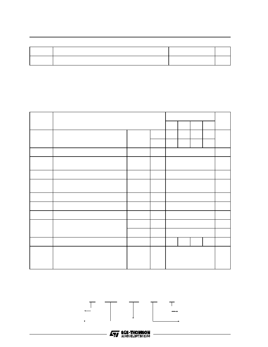
Symbol
Parameter
Value
Unit
I
T(RMS)
*
RMS on-state current
(180
∞
conduction angle)
Ta= 25
∞
C
0.26
A
I
T(AV)
*
Mean on-state current
(180
∞
conduction angle)
Ta= 25
∞
C
0.17
A
I
TSM
Non repetitive surge peak on-state current
(T
j
initial = 25
∞
C )
tp = 8.3 ms
7.5
A
tp = 10 ms
7
I
2
t
I
2
t Value for fusing
tp = 10 ms
0.24
A
2
s
dI/dt
Critical rate of rise of on-state current
I
G
= 10 mA
di
G
/dt = 0.1 A/
µ
s.
30
A/
µ
s
T
stg
T
j
Storage and operating junction temperature range
- 40, + 150
- 40, + 125
∞
C
Tl
Maximum lead temperature for soldering during 10s
260
∞
C
* : Mounted on a ceramic substrate of 8 x 10 x 0.7mm.
ABSOLUTE RATINGS (limiting values)
SOT23
(Plastic)
I
T(RMS)
= 0.2A
V
DRM
= 100V to 400V
Low I
GT
< 1
µ
A max to < 200
µ
A
FEATURES
Symbol
Parameter
Voltage
Unit
A
B
C
D
V
DRM
V
RRM
Repetitive peak off-state voltage
T
j
= 125
∞
C R
GK
= 1K
100
200
300
400
V
The P01xxxL series
of SCRs uses a high
performance planar PNPN technology. These
parts are intended for general purpose high
volume
applications using
surface
mount
technology.
DESCRIPTION
K
G
A
1/6
P
G (AV)
= 0.02 W P
GM
= 1 W (tp = 20
µ
s)
I
GM
= 0.5 A (tp = 20
µ
s)
GATE CHARACTERISTICS (maximum values)
Symbol
Parameter
Value
Unit
Rth(j-a)
Junction to ambient *
500
∞
C/W
* : Mounted on a ceramic substrate of 8 x 10 x 0.7mm.
THERMAL RESISTANCES
Symbol
Test Conditions
Sensitivity
Unit
02
09
11
15
I
GT
V
D
=12V (DC) R
L
=140
Tj= 25
∞
C
MIN
-
-
4
15
µ
A
MAX
200
1
25
50
V
GT
V
D
=12V (DC) R
L
=140
Tj= 25
∞
C
MAX
0.8
V
V
GD
V
D
=V
DRM
R
L
=3.3k
R
GK
= 1 K
Tj= 125
∞
C
MIN
0.1
V
V
RGM
I
RG
=10
µ
A
Tj= 25
∞
C
MIN
8
V
tgd
VD
=V
DRM
I
TM
= 3 x I
T(AV
)
dI
G
/dt = 0.1A/
µ
s
I
G
= 10mA
Tj= 25
∞
C
TYP
0.5
µ
s
I
H
I
T
= 50mA R
GK
= 1 K
Tj= 25
∞
C
MAX
5
mA
I
L
I
G
=1mA R
GK
= 1 K
Tj= 25
∞
C
MAX
6
mA
V
TM
I
TM
= 0.4A tp= 380
µ
s
Tj= 25
∞
C
MAX
1.3
V
I
DRM
I
RRM
V
D
= V
DRM
R
GK
= 1 K
V
R
= V
RRM
Tj= 25
∞
C
MAX
1
µ
A
Tj= 125
∞
C
MAX
100
µ
A
dV/dt
V
D
=67%V
DRM
R
GK
= 1 K
Tj= 125
∞
C
MIN
25
25
50
100
V/
µ
s
tq
I
TM
= 3 x I
T(AV
) V
R
=35V
dI/dt=10A/
µ
s
tp=100
µ
s
dV/dt=10V/
µ
s
V
D
= 67%V
DRM
R
GK
= 1 K
Tj= 125
∞
C
MAX
200
µ
s
ELECTRICAL CHARACTERISTICS
ORDERING INFORMATION
P
01
02
A
L
SCR PLANAR
CURRENT
PACKAGE :
L = SOT23
VOLTAGE
SENSITIVITY
Æ
P01xxxL
2/6

0.00
0.04
0.08
0.12
0.16
0.20
0.00
0.05
0.10
0.15
0.20
0.25
P (W)
360
O
= 180
o
= 120
o
= 90
o
= 60
o
= 30
o
DC
I
(A)
T(AV)
Fig.1 : Maximum average power dissipation ver-
sus average on-state current.
0
10 20 30 40 50 60 70 80 90 100 110 120 130
0.00
0.05
0.10
0.15
0.20
0.25
I
(A)
T(AV)
= 180
o
Tamb ( C)
o
Fig.3 : Average on-state current versus tab tem-
perature.
Igt
Ih
10.0
9.0
8.0
7.0
6.0
5.0
4.0
3.0
2.0
1.0
0.0
-40
-20
0
20
40
60
80
100
120
140
Igt[Tj]
Igt[Tj=25 C]
o
Ih[Tj]
Ih[Tj=25 C]
o
Tj( C)
o
Fig.5 : Relative variation of gate trigger current and
holding current versus junction temperature.
0
20
40
60
80
100
120
140
0.00
0.05
0.10
0.15
0.20
0.25
P (W)
Rth (j-a )
Tamb ( C)
o
Fig.2 : Correlation between maximum average
power dissipation and maximum allowable tem-
perature (Tamb).
1E-3
1E-2
1E-1
1E +0
1E +1
1 E+2
0.01
0.10
1.00
Zth(j-a)/Rth(j-a)
tp (s )
Alumin e su bst rat e: 10 mm*8 mm*0. 5mm
Fig.4 : Relative variation of thermal impedance
junction to ambient versus pulse duration.
1
10
100
1,000
0
1
2
3
4
5
6
7
8
Tj initial = 25 C
o
Number of cycles
I
(A)
TSM
Fig.6 : Non repetitive surge peak on-state current
versus number of cycles.
Æ
P01xxxL
3/6

1
10
0.1
1
10
100
I
(A). I
2
t (A
2
s)
TSM
Tj initial = 25 C
o
ITSM
tp(ms)
I
2
t
Fig.7 : Non repetitive surge peak on-state current
for a sinusoidal pulse with width : tp
10ms, and
corresponding value of I
2
t.
0
0.5
1
1.5
2
2.5
3
3.5
4
4.5
5
5.5
0.1
1
10
I
(A)
TM
Tj ini tial
25 C
o
Tj max
V
(V)
TM
Tj max
Vto =0.95 V
Rt =0. 600
Fig.8 : On-state characteristics (maximum values).
1 .0 E+0 0 1. 0E+01 1.0 E+ 02 1. 0E+ 03 1 .0 E+0 4 1. 0E+05 1. 0E+ 06
0.1
1.0
5.0
Ih(Rgk)
Ih(Rgk=1k
)
Tj =25 C
o
Rgk( )
Fig.9 : Relative variation of holding current versus
gate-cathode resistance (typical values).
Æ
P01xxxL
4/6
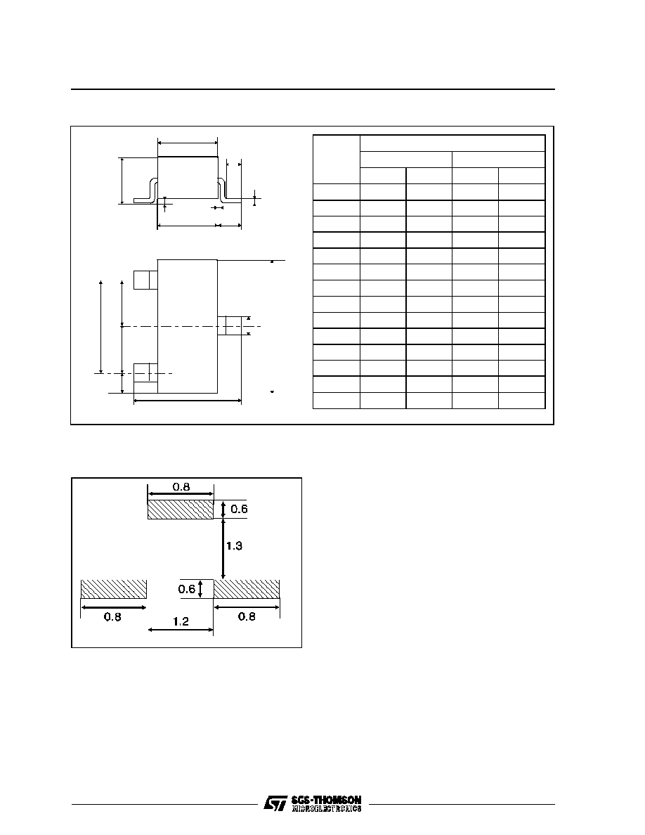
PACKAGE MECHANICAL DATA
SOT23 (Plastic)
B
B
E
A
G
F
C
D
J
I
H
L
K
M
N
REF.
DIMENSIONS
Millimeters
Inches
Min.
Max.
Min.
Max.
A
0.93
1.04
0.036
0.041
B
1.20
1.40
0.047
0.055
C
0.15
0.006
D
0.085
0.115
0.003
0.005
E
0.45
0.60
0.018
0.024
F
0.08
0.003
G
0.013
0.10
0.0005
0.004
H
1.90
2.05
0.075
0.081
I
0.95
1.05
0.037
0.041
J
0.95
1.05
0.037
0.041
K
2.10
2.50
0.083
0.098
L
0.45
0.60
0.018
0.024
M
0.37
0.46
0.015
0.018
N
2.80
3.00
0.110
0.118
Weight : 0.007 g
FOOT PRINT
Æ
P01xxxL
5/6