Æ
1/7
Table 1: Main Features
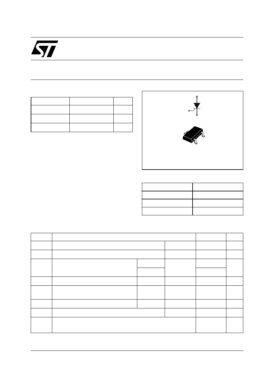
DESCRIPTION
Thanks to highly sensitive triggering levels, the
P01xxxL SCR series is suitable for all applications
where the available gate current is limited such as
stand-by mode power supplies, smoke and alarm
detectors...
Available in SOT23-3L, it provides optimized
space saving on high density printed circuit
boards.
Symbol
Value
Unit
I
T(RMS)
0.25
A
V
DRM
/V
RRM
100 and 200
V
I
GT
1 and 200
µA
P01xxxL
0.25A SCR
S
REV. 4
April 2005
SENSITIVE
Table 2: Order Codes
Part Numbers
Marking
P0102AL 5AA4
P2A
P0102BL 5AA4
P2B
P0109AL 5AA4
P9A
A
K
G
A
K
G
SOT23-3L
Table 3: Absolute Ratings (limiting values)
Symbol
Parameter
Value
Unit
I
T(RMS)
RMS on-state current (180∞ conduction angle)
T
amb
= 36∞C
0.25
A
IT
(AV)
Average on-state current (180∞ conduction angle)
T
amb
= 36∞C
0.16
A
I
TSM
Non repetitive surge peak on-state
current
t
p
= 8.3 ms
T
j
= 25∞C
7
A
t
p
= 10 ms
6
I
≤
t
I
≤
t Value for fusing
t
p
= 10 ms
T
j
= 25∞C
0.18
A
2S
dI/dt
Critical rate of rise of on-state current
I
G
= 2 x I
GT
, t
r
100 ns
F = 60 Hz
T
j
= 125∞C
50
A/µs
I
GM
Peak gate current
t
p
= 20 µs
T
j
= 125∞C
0.5
A
P
G(AV)
Average gate power dissipation
T
j
= 125∞C
0.02
W
T
stg
T
j
Storage junction temperature range
Operating junction temperature range
- 40 to + 150
- 40 to + 125
∞C
P01xxxL
2/7
Tables 4: Electrical Characteristics (T
j
= 25∞C, unless otherwise specified)
Table 5: Thermal resistance
Symbol
Test Conditions
P0102xL
P0109AL
Unit
I
GT
V
D
= 12 V R
L
= 140
MAX.
200
1
µA
V
GT
MAX.
0.8
V
V
GD
V
D
= V
DRM
R
L
= 3.3 k
R
GK
= 1 k
T
j
= 125∞C
MIN.
0.1
V
V
RG
I
RG
= 10 µA
MIN.
8
V
I
H
I
T
= 50 mA R
GK
= 1 k
MAX.
6
mA
I
L
I
G
= 1 mA R
GK
= 1 k
MAX.
7
mA
dV/dt
V
D
= 67 % V
DRM
R
GK
= 1 k
T
j
= 125∞C
MIN.
200
100
V/µs
V
TM
I
TM
= 0.4 A tp = 380 µs
T
j
= 25∞C
MAX.
1.7
V
V
t0
Threshold voltage
T
j
= 125∞C
MAX.
1.0
V
R
d
Dynamic resistance
T
j
= 125∞C
MAX.
1000
m
I
DRM
I
RRM
V
DRM
= V
RRM
T
j
= 25∞C
MAX.
1
µA
T
j
= 125∞C
100
Symbol
Parameter
Value
Unit
R
th(j-a)
Junction to ambient (mounted on FR4 with recommended pad layout)
400
∞C/W
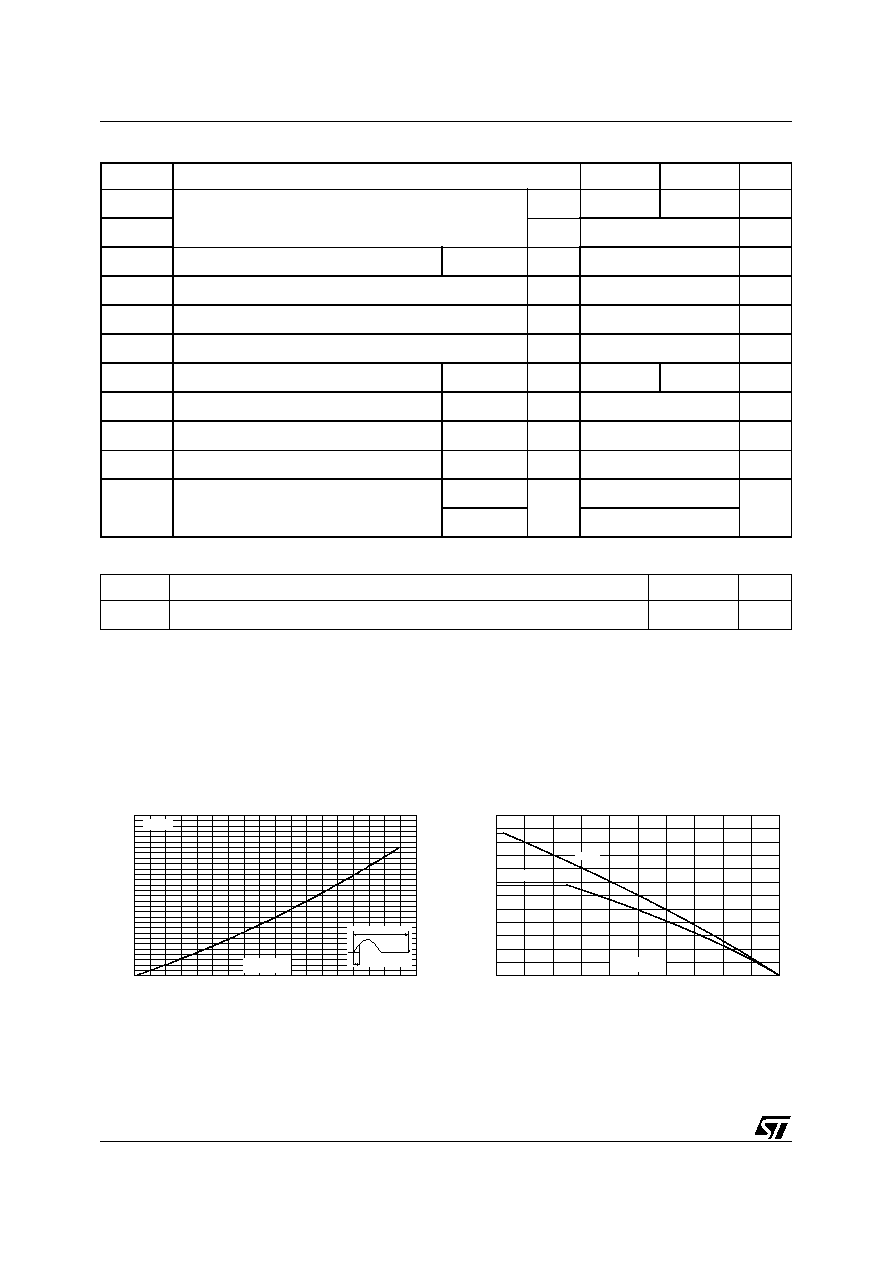
Figure 1: Maximum average power dissipation
versus average on-state current
Figure 2: Average and D.C. on-state current
versus case temperature
0.00
0.02
0.04
0.06
0.08
0.10
0.12
0.14
0.16
0.18
0.00
0.02
0.04
0.06
0.08
0.10
0.12
0.14
0.16
0.18
0.20
0.22
0.24
0.26
0.28
0.30
P(W)
I
(A)
T(AV)
= 180∞
360∞
0
25
50
75
100
125
0.00
0.05
0.10
0.15
0.20
0.25
0.30
I
(A)
T(AV)
T
(∞C)
case
= 180∞
D.C.

P01xxxL
3/7
Figure 3: Relative variation of thermal
impedance junction to ambient versus pulse
duration
Figure 4: Relative variation of gate trigger
current, holding current and latching current
versus junction temperature (typical values)
Figure 5: Relative variation of holding current
versus gate-cathode resistance (typical
values)
Figure 6: Relative variation of dV/dt immunity
versus gate-cathode resistance (typical
values)
Figure 7: Relative variation of dV/dt immunity
versus gate-cathode capacitance (typical
values)
Figure 8: Surge peak on-state current versus
number of cycles
1E-2
1E-1
1E+0
1E+1
1E+2
0.01
0.10
1.00
K=[Z
/R
th(j-a)
th(j-a)
]
t (s)
p
-40
-20
0
20
40
60
80
100
120
140
0
1
2
3
4
5
6
T (∞C)
j
I
,I ,I [T ] /
GT H L
j
I
,I ,I [T =25∞C]
GT H L
j
I
GT
I
H
& I
R
= 1k
L
GK
1E-2
1E-1
1E+0
1E+1
0
2
4
6
8
10
12
14
16
18
20
R
(k )
GK
I [R
] / I [
=1k ]
H
GK
H
R
GK
T
j
= 25∞C
0
200
400
600
800
1000
1200
1400
1600
1800
2000
0.1
1.0
10.0
R
(k )
GK
dV/dt[R
] / dV/dt[
=1k ]
GK
R
GK
T
j
= 125∞C
V = 0.67 x V
D
DRM
0
1
2
3
4
5
6
7
0
2
4
6
8
10
C
(nF)
GK
dV/dt[C
] / dV/dt[
=1k ]
GK
R
GK
T
V = 0.67 x V
= 125∞C
R
= 1k
D
DRM
GK
j
1
10
100
1000
0
1
2
3
4
5
6
7
I
(A)
TSM
Number of cycles
Non repetitive
T initial=25∞C
j
Repetitive
T
=25∞C
amb
t =10ms
p
One cycle
P01xxxL
4/7
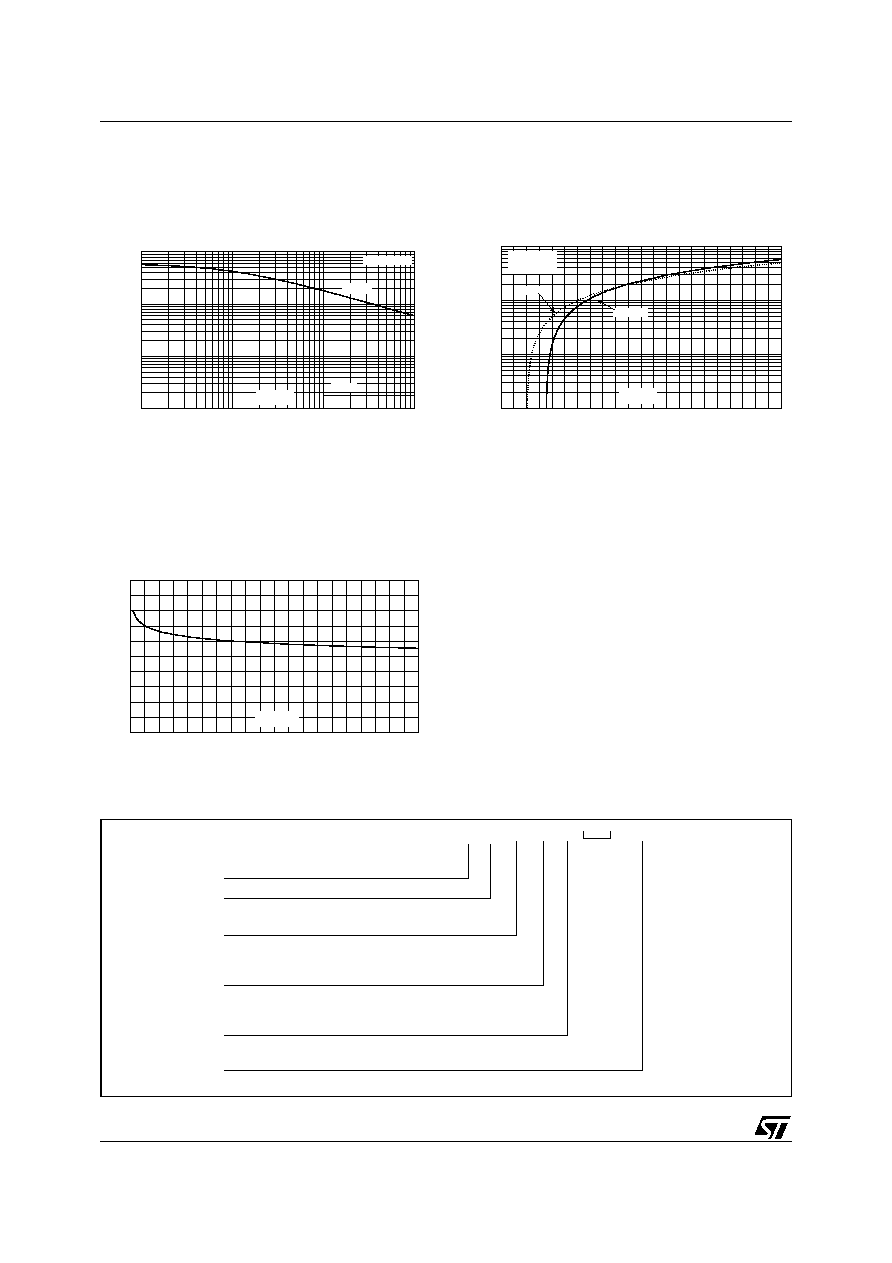
Figure 12: Ordering Information Scheme
Figure 9: Non-repetitive surge peak on-state
current for a sinusoidal pulse with width t
p
< 10ms,
and corresponding value of I≤t
Figure 10: On-state characteristics (maximum
values)
Figure 11: Thermal resistance junction to
ambient versus copper surface under tab
(Epoxy printed circuit board FR4, copper
thickness: 35 mm)
0.01
0.10
1.00
10.00
0.1
1.0
10.0
100.0
I
(A), I t (A s)
TSM
2
2
t (ms)
p
I t
2
I
TSM
T initial = 25∞C
j
0.5
1.0
1.5
2.0
2.5
3.0
3.5
4.0
4.5
5.0
5.5
6.0
1E-2
1E-1
1E+0
1E+1
I
(A)
TM
V
(V)
TM
T
j
=max
T =25∞C
j
V =1.0V
R =1
T max.:
j
t0
d
0
10
20
30
40
50
60
70
80
90
100
0
100
200
300
400
500
S(cm≤)
R
(∞C/W)
th(j-a)
P 01 02 A L
5AA4
Blank
Sensitive SCR series
Sensitivity
Voltage
Package
Packing mode
Current
01 = 0.25A
02 = 200µA
09 = 1µA
A = 100V
B = 200V
L = SOT23-3L
5AA4 = Tape & Reel

P01xxxL
5/7
Table 6: Product Selector
Figure 13: SOT23-3L Package Mechanical Data
Figure 14: Foot Print Dimensions (in millimeters)
Part Number
Voltage
Sensitivity
Package
P0102AL 5AA4
100 V
200 µA
SOT23-3L
P0102BL 5AA4
200 V
200 µA
P0109AL 5AA4
100 V
1 µA
A1
A
L
H
B
E
D
e
e1
S
c
0.95
0.61
1.26
3.25
0.73
REF.
DIMENSIONS
Millimeters
Inches
Min.
Max.
Min.
Max.
A
0.89
1.4
0.035
0.055
A1
0
0.1
0
0.004
B
0.3
0.51
0.012
0.02
c
0.085
0.18
0.003
0.007
D
2.75
3.04
0.108
0.12
e
0.85
1.05
0.033
0.041
e1
1.7
2.1
0.067
0.083
E
1.2
1.6
0.047
0.063
H
2.1
2.75
0.083
0.108
L
0.6 typ.
0.024 typ.
S
0.35
0.65
0.014
0.026