 | –≠–ª–µ–∫—Ç—Ä–æ–Ω–Ω—ã–π –∫–æ–º–ø–æ–Ω–µ–Ω—Ç: TD350IDT | –°–∫–∞—á–∞—Ç—å:  PDF PDF  ZIP ZIP |

August 2004
Revision 1
1/11
s
0.75A source/1.2A sink min gate drive
s
Active Miller clamp feature
s
Two steps turn-off with adjustable level
and delay
s
Desaturation detection
s
Fault status output
s
Negative gate drive ability
s
Input compatible with pulse transformer or
optocoupler
s
Separate sink and source outputs for easy
gate drive
s
UVLO protection
s
2kV ESD protection
Description
TD350 is an advanced gate driver for IGBT and
power MOSFET. Control and protection functions
are included and allow the design of high reliability
systems.
Innovative active Miller clamp function avoids the
need of negative gate drive in most applications
and allows the use of a simple bootstrap supply
for the high side driver
TD350 includes a two-level turn-off feature with
adjustable level and delay. This function protects
against excessive overvoltage at turn-off in case
of overcurrent or short-circuit condition. Same
delay is applied at turn-on to prevent pulse width
distortion.
TD350 also includes an IGBT desaturation
protection and a FAULT status output.
TD350 is compatible with both pulse transformer
and optocoupler signals.
Applications
s
1200V 3-Phase Inverter
s
Motor C
ontrol
s
UPS Systems
Pin Connections (top view)
Order Codes
D
SO-14
(Plastic MicroPackage)
COFF
IN
LVOFF
OUTH
VH
DESAT
TD350
NC
NC
FAULT
CLAMP
OUTL
GND
VREF
VL
5
1
2
6
4
3
7
10
14
13
9
11
12
8
Part Number
Temperature Range
Package
Packaging
TD350ID
-40, +125∞C
SO
Tube
TD350IDT
Tape & Reel
TD350
Advanced IGBT/MOSFET Driver
TD350
Block Diagram
2/11
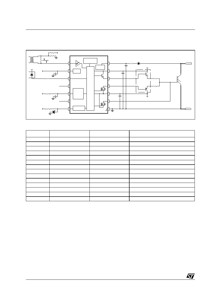
1 Block Diagram
Figure 1: Schematic block diagram
Table 1: Pin description
Name
Pin Number
Type
Function
IN
1
Analog input
Input
VREF
2
Analog output
+5V reference voltage
FAULT
3
Digital output
Fault status output
NC
4
Not connected
COFF
5
Timing capacitor
Turn off delay
NC
6
Not connected
LVOFF
7
Analog input
Turn off level
GND
8
Power supply
Signal ground
CLAMP
9
Analog output
Miller clamp
VL
10
Power supply
Negative supply
OUTL
11
Analog output
Gate drive output (sink)
OUTH
12
Analog output
Gate drive output (source)
VH
13
Power supply
Positive supply
DESAT
14
Analog input
Desaturation protection
OUTH
IN
Vref
OUTL
VH
DESAT
TD350
C
ont
r
o
l
Bl
o
c
k
FAULT
NC
COFF
CLAMP
GND
16V
Desat
Pulse Transformer
delay
Off
VREF
VL
-10V
Optionnal
Vref
Vref
LVOFF
VH
Off Level
UVLO
Vref
NC
VH

Absolute Maximum Ratings
TD350
3/11
2 Absolute Maximum Ratings
Table 2: Key parameters and their absolute maximum ratings
Symbol
Parameter
Value
Unit
VHL
Maximum Supply Voltage (VH - VL)
28
V
VH
Maximum VH voltage vs. GND
28
V
VL
Minimum VL voltage vs. GND
-12
V
Vout
Voltage on OUTH, OUTL, CLAMP pins
VL-0.3 to VH+0.3
V
Vdes
Voltage on DESAT, FAULT, LVOFF pin
-0.3 to VH+0.3
V
Vter
Voltage on other pins (IN, COFF, VREF)
-0.3 to 7
V
Pd
Power dissipation
500
mW
Tstg
Storage temperature
-55 to 150
∞C
Tj
Maximum Junction Temperature
150
∞C
Rhja
Thermal Resistance Junction-Ambient
125
∞C/W
Rhjc
Thermal Resistance Junction-Case
22
∞C/W
ESD
Electrostatic discharge
2
kV
Table 3: Operating conditions
Symbol
Parameter
Value
Unit
VH
Positive Supply Voltage vs. GND
UVLO to 26
V
VL
Negative Supply Voltage vs. GND
0 to -10
V
VH-VL
Maximum Total Supply Voltage
26
V
Toper
Operating Free Air Temperature Range
-40 to 125
∞C

TD350
Electrical Characteristics
4/11
3 Electrical Characteristics
Table 4: T
amb
= -20 to 125∞C, VH=16V, VL=-10V (unless otherwise specified)
Symbol
Parameter
Test Condition
Min
Typ
Max
Unit
Input
Vton
IN turn-on threshold voltage
0.8
1.0
V
Vtoff
IN turn-off threshold voltage
4.0
4.2
V
tonmin
Minimum pulse width
100
135
220
ns
Iinp
IN Input current
1
µ
A
Voltage reference - note
1
1)
Recommended capacitor range on VREF pin is 10nF to 100nF.
Vref
Voltage reference
T=25∞C
Tmin<T<Tmax
4.85
4.77
5.00
5.15
5.22
V
V
Iref
Maximum output current
10
mA
Desaturation protection
Vdes
Desaturation threshold
6.5
7.2
7.9
V
Ides
Source current
250
µ
A
Fault output
tfault
Delay for fault detection
500
ns
VFL
FAULT low voltage
Ifsink=10mA
1
V
Clamp
Vtclamp
CLAMP pin voltage threshold
2.0
V
VCL
Clamp low voltage at Icsink=500mA
T=25∞C
Tmin<T<Tmax
VL+2.5
VL+3.0
V
V
Off Delay
Vtdel
Voltage threshold
2.35
2.50
2.65
V
Rdel
Discharge resistor
I=1mA
500
Off Levels
Iblvoff
LVOFF peak input current (sink)
LVOFF=12V
120
200
µ
A
Violv
Offset voltage
LVOFF=12V
-0.3
-0.15
0
V
Outputs
VOL1
Output low voltage at Iosink=20mA
VL+0.35
V
VOL2
Output low voltage at Iosink=200mA
T=25∞C
Tmin<T<Tmax
VL+1.0
VL+1.5
V
V
VOL3
Output low voltage at Iosink=500mA
T=25∞C
Tmin<T<Tmax
VL+2.5
VL+3.0
V
V
VOH1
Output high voltage 1
Iosource=20mA
VH-2.5
V
VOH2
Output high voltage 2
Iosource=200mA
VH-3.0
V
VOH3
Output high voltage 3
Iosource=500mA
VH-4.0
V
tr
Rise time
CL=1nF, 10% to 90%
VL=0
VL=-10V
130
175
ns
ns
tf
Fall time
(2 step turn-off disabled)
CL=1nF, 90% to 10%
VL=0
VL=-10V
75
90
ns
ns
tpd
Input to output propagation delay at
turn-on (2 step delay disabled)
10% output change
270
800
ns
tw
Input to output pulse distortion
10% output change
10
60
110
ns
Under Voltage Lockout (UVLO)
UVLOH
UVLO top threshold
10
11
12
V
UVLOL
UVLO bottom threshold
9
10
11
V
Vhyst
UVLO hysteresis
UVH-UVL
0.5
1
V
Supply current
Iin
Quiescent current
output=0V, no load
5
mA

Functional Description
TD350
5/11
4 Functional
Description
4.1 Input
The input is compatible with optocouplers or pulse
transformers. The input is triggered by the signal
edge and allows the use of low-sized, low-cost
pulse transformer. Input is active low (output is
high when input is low) to ease the use of
optocoupler. When driven by a pulse transformer,
the input pulse (positive and negative) width must
be larger than the minimum pule width t
onmin
.
4.2 Voltage reference
A voltage reference is used to create accurate
timing for the two-level turn-off with external
resistor and capacitor.
4.3 Desaturation protection
Desaturation protection ensures the protection of
the IGBT in the event of overcurrent. When the
DESAT voltage goes higher that 7V, the output is
driven low (with 2-level turn-off if applicable). The
FAULT output is activated. The FAULT state is
exited at the next falling edge of IN input.
A programmable blanking time is used to allow
enough time for IGBT saturation. Blanking time is
provided by an internal current source and
external capacitor.
DESAT input can also be used with an external
comparator for overcurrent or over temperature
detection.
4.4 Active Miller clamp
A Miller clamp allows the control of the Miller
current during a high dV/dt situation and can avoid
the use of a negative supply voltage.
During turn-off, the gate voltage is monitored and
the clamp output is activated when gate voltage
goes below 2V (relative to GND). The clamp
voltage is VL+3V max for a Miller current up to
500mA. The clamp is disabled when the IN input
is triggered again.
4.5 Two level turn-off
The two-level turn-off is used to increase the
reliability of the application.
During turn-off, gate voltage can be reduced to a
programmable level in order to reduce the IGBT
current (in the event of over-current). This action
avoids both dangerous overvoltage across the
IGBT, and RBSOA problems, especially at short
circuit turn-off.
Turn-off (T
a
) delay is programmable through an
external resistor and capacitor for accurate timing.
Turn-off delay (T
a
) is also used to delay the input
signal to prevent distortion of input pulse width.
4.6 Minimum ON time
In order to ensure the proper operation of the 2-
level turn-off function, the input ON time (T
win
)
must be greater than the T
winmin
value:
T
winmin
=T
a
+2*R
del
*C
off
R
del
is the internal discharge resistor and C
off
is
the external timing capacitor.
Input signals smaller than Ta are ignored. Input
signals larger than T
winmin
are transmitted to the
output stage after the T
a
delay with minimum
width distortion (
T
w
=T
wout
-T
win
).
For an input signal width T
win
between T
a
and
T
winmin
, the output width T
wout
is reduced below
T
win
(pulse distortion) and the IGBT could be
partially turned on. These input signals should be
avoided during normal operation.
4.7 Output
The output stage is able to sink 2.3A and source
1.5A typical at 25∞C (1.2A/0.75A minimum over
the full temperature range). Separated sink and
source outputs allow independent gate charge
and discharge control without an extra external
diode.