November 2004
revision 1
1/12
s
1A sink / 0.75A source min. gate drive
s
Active Miller clamp feature
s
Adjustable and accurate two steps turn-off
level and delay
s
Input compatible with pulse transformer or
optocoupler
s
UVLO protection
s
2kV ESD protection
Description
TD351 is an advanced gate driver for IGBT and
power MOSFET. Control and protection functions
are included and allow the design of high reliability
systems
Innovative active Miller clamp function avoids the
need of negative gate drive in most applications
and allows the use of a simple bootstrap supply
for the high side driver
TD351 includes a two-level turn-off feature with
adjustable level and delay. This function protects
against excessive overvoltage at turn-off in case
of overcurrent or short-circuit condition. Same
delay is applied at turn-on to prevent pulse width
distortion.
TD351 is compatible with both pulse transformer
and optocoupler signals.
Applications
s
1200V 3-phase inverter
s
Motor control systems
s
UPS
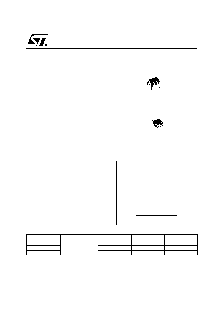
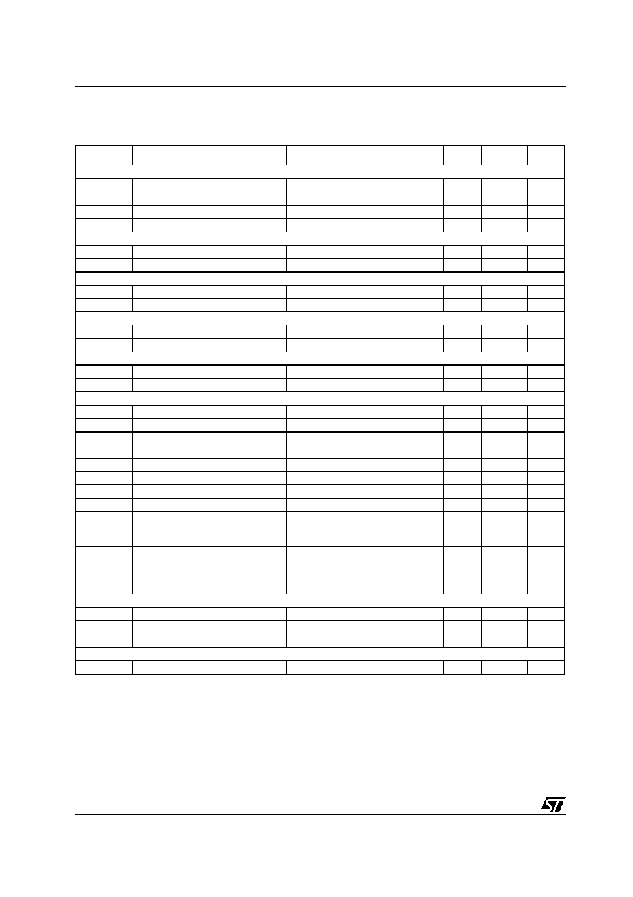
Pin Connections (top view)
Order Codes
D
SO-8
(Plastic Micropackage)
N
DIP-8
(Plastic Package)
VREF
VH
IN
TD351
CD
VL
LVOFF
OUT
CLAMP
2
1
3
4
7
8
6
5
Part Number
Temperature Range
Package
Packaging
Marking
TD351IN
-40∞C, +125∞C
DIP
Tube
TD351I
TD351ID
SO
Tube
TD351I
TD351IDT
SO
Tape & Reel
TD351I
TD351
Advanced IGBT/MOSFET Driver

Absolute Maximum Ratings
TD351
3/12
2 Absolute
Maximum
Ratings
Table 2: parameters and their absolute maximum ratings
Table 3: Operating Conditions
Symbol
Parameter
Value
Unit
VHL
Maximum Supply Voltage (VH - VL)
28
V
Vout
Voltage on OUT, CLAMP, LVOFF pins
VL-0.3 to VH+0.3
V
Vter
Voltage on other pins (IN, CD, VREF)
-0.3 to 7
V
Pd
Power dissipation
500
mW
Tstg
Storage temperature
-55 to 150
∞C
Tj
Maximum Junction Temperature
150
∞C
Rhja
Thermal Resistance Junction-Ambient
150
∞C/W
ESD
Electrostatic discharge
2
kV
Symbol
Parameter
Value
Unit
VH
Positive Supply Voltage vs. VL
UVLO to 26
V
Toper
Operating Free Air Temperature Range
-40 to 125
∞C
TD351
Electrical Characteristics
4/12
3 Electrical
Characteristics
Table 4: Electrical characteristics for T
amb
= -20 to 125∞C, VH=16V (unless otherwise specified)
Note: 1.Recommended capacitor range on VREF pin is 10nF to 100nF
Symbol
Parameter
Test Condition
Min
Typ
Max
Unit
Input
Vton
IN turn-on threshold voltage
0.8
1.0
V
Vtoff
IN turn-off threshold voltage
4.0
4.2
V
tonmin
Minimum pulse width
100
135
220
ns
Iinp
IN Input current
IN input voltage < 4.5V
1
µ
A
Voltage reference - Note 1
Vref
Voltage reference
T=25∞C
4.85
5.00
5.15
V
Iref
Maximum output current
10
mA
Clamp
Vtclamp
CLAMP pin voltage threshold
2.0
V
VCL
Clamp low voltage
Icsink=500mA
2.5
V
Delay
Vtdel
Voltage threshold
2.5
V
Rdel
Discharge resistor
I=1mA
500
Off Level
Iblvoff
LVOFF peak input current (sink)
LVOFF=12V
90
200
µ
A
Violv
Offset voltage
LVOFF=12V
-0.3
-0.15
0
V
Outputs
Isink
Output sink current
Vout=6V
1000
1700
mA
Isrc
Output source current
Vout=VH-6V
750
1300
mA
VOL1
Output low voltage 1
Iosink=20mA
0.35
V
VOL2
Output low voltage 2
Iosink=500mA
2.5
V
VOH1
Output high voltage 1
Iosource=20mA
VH-2.5
V
VOH2
Output high voltage 2
Iosource=500mA
VH-4.0
V
tr
Rise time
CL=1nF, 10% to 90%
100
ns
tf
Fall time (2 step turn-off disabled)
CL=1nF, 90% to 10%
100
ns
tdon
Turn on propagation delay
10% output change:
Rd=4.7k, no Cd
Rd=10k, Cd=220pF
1.8
2.0
600
2.2
ns
µ
s
tdoff
Turn off propagation delay
(2-level turn-off disabled)
10% output change
550
ns
tw
Input to output pulse distortion
10% output change,
tw=Twout-Twin
50
100
ns
Under Voltage Lockout (UVLO)
UVLOH
UVLO top threshold
10
11
12
V
UVLOL
UVLO bottom threshold
9
10
11
V
Vhyst
UVLO hysteresis
Vhyst=UVLOH-UVLOL
0.5
1
V
Supply current
Iin
Quiescent current
input low, no load
2.5
mA

Functional Description
TD351
5/12
4 Functional
Description
4.1 Input stage
TD351 input is compatible with optocouplers or
pulse transformers. The input is triggered by the
signal edge and allows the use of low-sized, low-
cost pulse transformer. Input is active low: output
is driven high when input is driven low. The IN
input is internally clamped at about 5V to 7V.
When using an open collector optocoupler, the
resistive pull-up resistor can be connected to
either VREF or VH. Recommended pull-up
resistor value with VH=16V are from 4.7k to 22k.
When driven by a pulse transformer, the input
positive and negative pulse widths at the Vton and
Vtoff threshold voltages must be larger than the
minimum pulse width t
onmin
(see fig. 4). This
feature acts as a filter against invalid input pulses
smaller than t
onmin
.
4.2 Voltage reference
A voltage reference is used to create accurate
timing for the turn-on delay with external resistor
and capacitor. The same circuitry is also used for
the two-level turn-off delay.
A decoupling capacitor (10nF to 100nF) on VREF
pin is required to ensure good noise rejection.
4.3 Active Miller clamp:
The TD351 offers an alternative solution to the
problem of the Miller current in IGBT switching
applications. Instead of driving the IGBT gate to a
negative voltage to increase the safety margin,
the TD351 uses a dedicated CLAMP pin to control
the Miller current. When the IGBT is off, a low
impedance path is established between IGBT
gate and emitter to carry the Miller current, and
the voltage spike on the IGBT gate is greatly
reduced.
During turn-off, the gate voltage is monitored and
the clamp output is activated when gate voltage
goes below 2V (relative to VL). The clamp voltage
is VL+4V max for a Miller current up to 500mA.
The clamp is disabled when the IN input is
triggered again.
The CLAMP function doesn't affect the turn-off
characteristic, but only keeps the gate to the low
level throughout the off time. The main benefit is
that negative voltage can be avoided in many
cases, allowing a bootstrap technique for the high
side driver supply.
4.4 Two level turn-off
During turn-off, gate voltage can be reduced to a
programmable level in order to reduce the IGBT
current (in the event of over-current). This action
avoids both dangerous overvoltage across the
IGBT, and RBSOA problems, especially at short
circuit turn-off.
Turn-off (T
a
) delay is programmable through
external resistor R
d
and capacitor C
d
for accurate
timing. T
a
is approximately given by:
T
a
(µs) = 0.7. R
d
(kOhms). C
d
(nF)
Turn-off delay (T
a
) is also used to delay the input
signal to prevent distortion of input pulse width.
The Two level turn-off sequence can be disabled
by connecting LVOFF pin to VH and connecting
CD pin to VREF with a 4.7k resistor.
4.5 Minimum Input ON-time
Input signals with ON-time smaller than T
a
are
ignored. ON-time signals larger than T
a
+2.R
del
.C
d
(R
del
is the internal discharge switch resistance,
C
d
is the external timing capacitor) are transmitted
to the output stage after the T
a
delay with
minimum width distortion (
T
w
=T
wout
-T
win
). For
ON-time input signals close to T
a
(between T
a
and
T
a
+2.R
del
.C
d
), the 2-level duration is slightly
reduced and the total output width can be smaller
than the input width (see fig. 5).
4.6 Output stage
The output stage is able to sink/source 1.7A/1.3A
typical at 25∞C and 1.0A/0.75A min. over the full
temperature range. This current capability is
specified near the usual IGBT Miller plateau.
4.7 Undervoltage protection
Undervoltage detection protects the application in
the event of a low VH supply voltage (during start-
up or a fault situation). During undervoltage, the
OUT pin is driven low (active pull-down for
VH>2V, passive pull-down for VH<2V.
VH
OUT
2V
UVH
UVL
Vccmin
FAULT
