
TDA1175P
LOW-NOISE VERTICAL DEFLECTION SYSTEM
August 1995
1
2
3
4
5
6
7
8
16
15
14
13
12
11
10
9
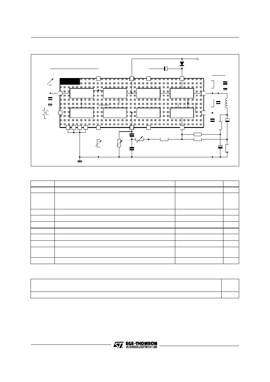
RAMP GENERATOR
COMPENSATION
AMP. INPUT
GROUND
GROUND
OSCILLATOR
SYNC. INPUT
HEIGHT ADJUSTMENT
RAMP OUTPUT
SUPPLY VOLTAGE
FLYBACK
GROUND
GROUND
POWER AMPLIFIER OUTPUT
POWER AMPLIFIER
SUPPLY VOLTAGE
REGULATED VOLTAGE
1175P-01.EPS
PIN CONNECTIONS
POWERDIP16
(Plastic Package)
ORDER CODE : TDA1175P
.
COMPLETE VERTICAL DEFLECTION
SYSTEM
.
LOW NOISE
.
SUITABLE FOR HIGH DEFINITION
MONITORS
.
ESD PROTECTED
DESCRIPTION
The TDA1175P is a monolithic integrated circuit in
POWERDIP16 plastic package. It is intended for
use in black and white and colour TV receivers.
Low-noise makes this device particularly suitable
for use in monitors.
The functions incorporated are : synchronization
circuit, oscillator and ramp generator, high power
gain amplifier, flyback generator, voltage regulator.
1/8
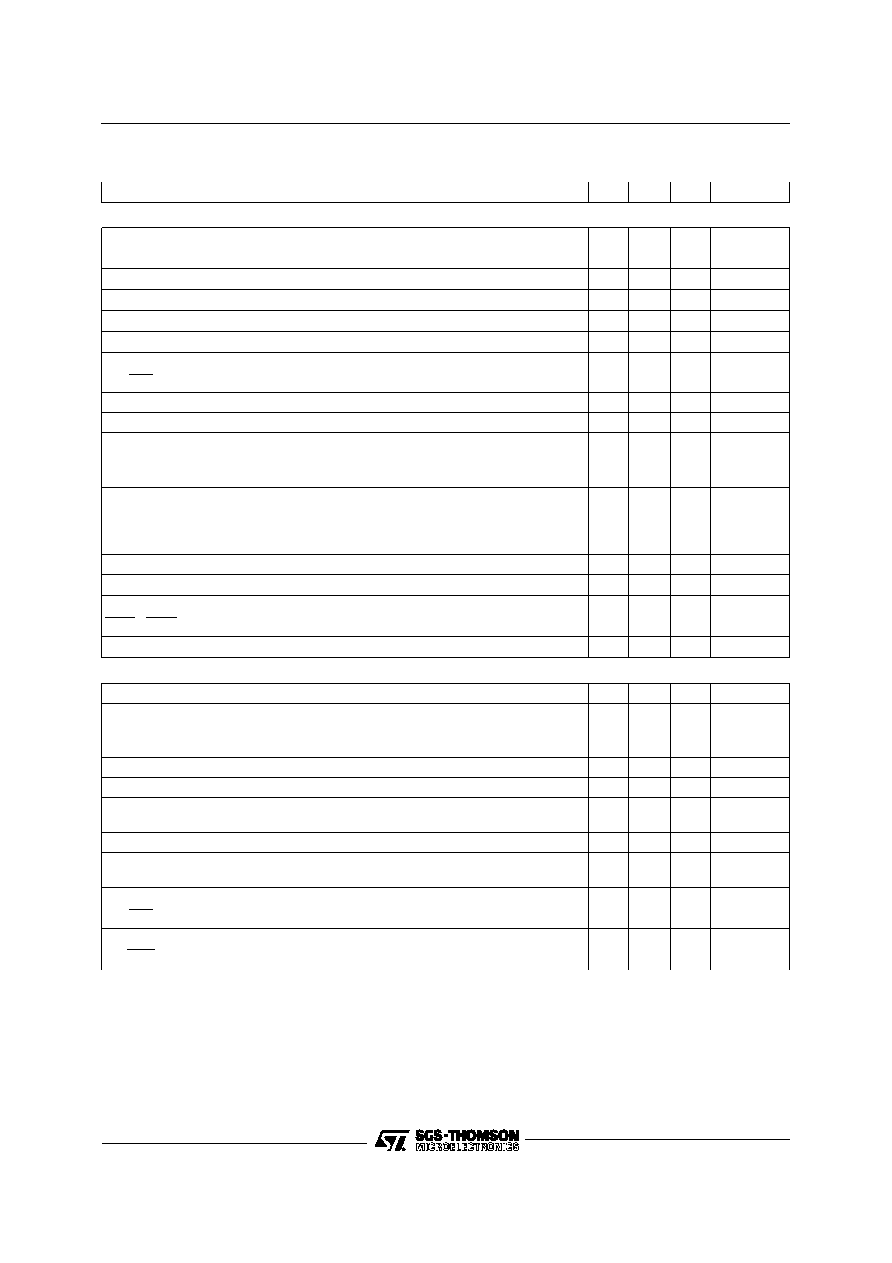
OSCILLATOR
VOLTAGE
REGULATOR
BUFFER
STAGE
SYNC
CIRCUIT
RAMP
GENERATOR
FLYBACK
GENERATOR
SYNC
YOKE
LINEARITY
TABS
HEIGHT
FREQ
C1
P3
P2
R
A
C
C3
2
R
R
B
C
R
D
R
E
R
F
C6
C7
C5
C8
C9
R
R
H
G
C4
D
A
+ V
S
8
11
10
2
9
16
1
14
15
6
3
7
POWER
AMPLIFIER
PREAMPLIFIER
P1
TDA1175P
12
5
4
13
1175P-02.EPS
BLOCK DIAGRAM
ABSOLUTE MAXIMUM RATINGS
Symbol
Parameter
Value
Unit
V
s
Supply Voltage at Pin 2
35
V
V
6
, V
7
Flyback Peak Voltage
60
V
V
14
Power Amplifier Input Voltage
+ 10
� 0.5
V
V
I
o
Output Peak Current (non repetitive) at t = 2ms
2
A
I
o
Output Peak Current at f = 50Hz, t
10
�
s
2.5
A
I
o
Output Peak Current at f = 50Hz, t > 10
�
s
1.5
A
I
3
Pin 3 DC Current at V
6
< V
2
100
mA
I
3
Pin 3 Peak to Peak Flyback Current for f = 50Hz, t
fly
1.5ms
1.8
A
I
10
Pin 10 Current
�
20
mA
P
to t
Power Dissipation : at T
ta b
= 90
�
C
at T
amb
= 70
�
C (free air) (1)
4.3
1
W
W
T
stg
, T
j
Storage and Junction Temperature
� 40, + 150
�
C
1175P-01.TBL
THERMAL DATA
Symbol
Parameter
Value
Unit
R
th (j-tab)
Thermal Resistance Junction-pin
Max.
12
�
C/W
R
th (j-amb)
Thermal Resistance Junction-ambient
Max.
80
�
C/W
(1)
1175P-02.TBL
(1) Obtained with tabs soldered to printed circuit with minimized copper area.
TDA1175P
2/8
ELECTRICAL CHARACTERISTICS (T
amb
= 25
�
C, unless otherwise specified)
Symbol
Parameter
Test Conditions
Min.
Typ.
Max.
Unit
Fig.
DC CHARACTERISTICS (Refer to the test circuits, V
S
= 35V)
I
2
Pin 2 Quiescent Current
I
3
= 0
7
14
mA
1b
I
7
Pin 7 Quiescent Current
I
6
= 0
8
17
mA
1b
� I
11
Oscillator Bias Current
V
11
= 1V
0.1
1
�
A
1a
� I
14
Amplifier Input Bias Current
V
14
= 1V
1
10
�
A
1b
� I
16
Ramp Generator Bias Current
V
16
= 0
0.02
0.3
�
A
1a
� I
16
Ramp Generator Current
I
9
= 20
�
A, V
16
= 0
18.5
20
21.5
�
A
1b
I
16
I
16
Ramp Generator Non-linearity
V
16
= 0 to 12V, I
9
= 20
�
A
0.2
1
%
1b
V
s
Supply Voltage Range
10
35
V
V
1
Pin 1 Saturation Voltage to Ground
I
1
= 1mA
1
1.4
V
V
3
Pin 3 Saturation Voltage to Ground
I
3
= 10mA
1.5
2.5
V
1a
V
6
Qiuescent output Voltage
V
s
= 10V, R1 = 1k
, R2 = 1k
V
s
= 35V, R1 = 3k
, R2 = 1k
4.1
8.2
4.4
8.8
4.7
9.4
V
V
1a
1a
V
6L
Output Saturation Voltage to
Ground
� I
6
= 0.1A
� I
6
= 0.8A
0.9
1.8
1.2
2.2
V
v
1c
1c
V
6H
Output Saturation Voltage to Supply I
6
= 0.1A
I
6
= 0.8A
1.4
2.8
2.1
3.1
V
V
1d
1d
V
8
Regulated Voltage at Pin 8
6.5
6.7
6.9
V
1b
V
9
Regulated Voltage at Pin 9
I
9
= 20
�
A
6.6
6.8
7
V
1b
|
V
8
|
V
S
,
|
V
9
|
V
S
Regulated Voltage Drift with Supply
Voltage
Vs = 10 to 35V
1
2
mV/V
1b
V
14
Amplifier Input Reference Voltage
V
10
0.4V
2.20
2.27
2.35
V
AC CHARACTERISTICS (Refer to the AC test circuit, V
S
= 22V, f = 50Hz)
I
s
Supply Current
I
y
= 1A
PP
140
mA
2
I
10
Sync. Input Current (positive or
negative)
0.5
2
mA
2
V
6
Flyback Voltage
I
y
= 1A
PP
45
V
2
t
fly
Flyback Time
I
y
= 1A
PP
0.7
ms
2
V
ON
Peak to Peak Output Noise
Pin 11 Connected to GND
18
30
mVpp
2
f
o
Free Running Frequency
(P1 + R1) = 300k
C9 = 0.1
�
F
36
43.5
Hz
2
f
OPER
Operating Frequency Range
10
120
Hz
2
f
Synchronization Range
I
10
= 0.5mA, C9 = 0.1
�
F
(P1+R1) = 300k
14
Hz
2
f
V
S
Frequency Drift with Supply Voltage V
s
= 10 to 35V
0.005
Hz/V
2
|
f
|
T
ab
Frequency Drift with tab
Temperature
T
tab
= 40 to 120
�
C
0.01
Hz/
�
C
2
1175P-03.TBL
TDA1175P
3/8

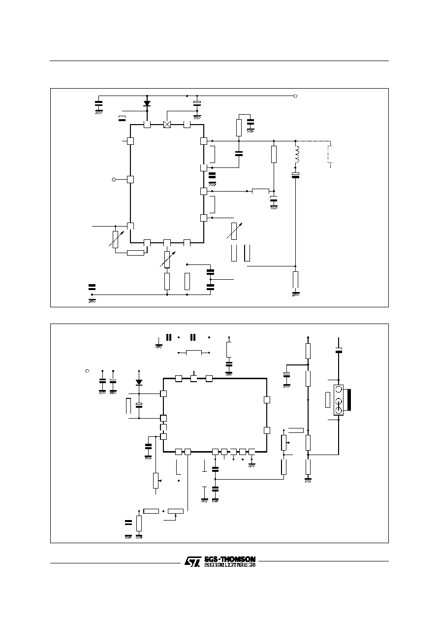
Figure 1 : DC Test Circuits
3
2
7
10
11
9
16
14
6
TABS
V
I
3
3
S
1V
1V
8V
1k
9
- I
- I
12
R2
R1
4
V
TDA1175P
+V
I
8
1175P-03.EPS
Figure 1a
2
7
11
16
14
TABS
I
S
1V
- I
12
V
TDA1175P
5
I
2
9
8
- I
V
6
7
10
100k
+V
1175P-04.EPS
Figure 1b
2
7
11
14
6
TABS
I
S
V
TDA1175P
+V
4L
4V
4
1175P-05.EPS
Figure 1c
2
7
11
14
6
TABS
S
V
TDA1175P
+V
4H
1V
I
4
1175P-06.EPS
Figure 1d
TDA1175P
4/8
1
2
3
6
7
8
9
10
11
14
15
16
22k
470pF
220k
910k
0.1
�
F
100k
47k
0.1
�
F
3.3
100pF
0.1
�
F
5.6k
10
�
F
5.6k
100k
120k
1.8k
P1
100k
220k
C9
0.1
�
F
Yoke
Ry = 10
Ly = 20mH
560
*
1000
�
F
1
SYNC.
INPUT
TABS
1N4001
470
�
F
100
�
F
0.1
�
F
V
= 22V
S
* on application only
TDA1175P
R1
1175P-07.EPS
Figure 2 : AC Test and Application Circuit for Large Screen B/W TV Set 10
/20mH/1A
PP
1
2
3
4
5
6
7
10
16
11
12
13
15
C6
0.1
�
F
C7
0.1
�
F
R4
1M
9
R2
82k
P1
100k
8
C4
0.15
�
F
C3
100
�
F
35V
R1
3.3k
D1
1N4007
C2
1000
�
F
35V
C1
0.1
�
F
V
(26V)
S
R12
220k
C9
C10 560pF
3.3nF
TDA1175P
R13
3. 3
C11
0. 1
�
F
P3
50k
V.LIN
R6
56k
R8
47k
R10
0.82
R9
5.1k
14
R11
R7
2.7k
27k
C8
22
�
F
35V
R3
240k
C5
1.8nF
V. SIZE
P2
220k
R5
200k
V. FREQ
Y1
YOKE
R14
220
1/2W
C12
470
�
F
50V
1175P-08.EPS
Figure 3 : Typical Application Circuit for VGA Monitor (R
Y
= 10
, L
Y
= 20mH, I
Y
= 0.8A
PP
)
TDA1175P
5/8

P2
R6
C2
R9
C6
R2
GN D
P1
C4
R11
R18
R12
C18
C9
C12
V-FREQ
V-SIZE
V S
C1
C3
P3
V.LIN
R14
R7
C7
R4
R8
C8
R10
Y1
C11
D1
R1
IC1
C6
R8
R6
R
1175P-09.EPS
Figure 4 : P.C. Board and Components Layout of the Circuit of Figure 3 (1:1 scale)
Item
Qty
Reference
Part
1
4
C1, C6, C7, C11
0.1
�
F
2
1
C2
1000
�
F 35V
3
1
C3
100
�
F 35V
4
1
C4
0.15
�
F
5
1
C5
1.8nF
6
1
C8
22
�
F 35V
7
1
C9
3.3nF
8
1
C10
560pF
9
1
C12
470
�
F 50V
10
1
D1
1N4007
11
1
IC1
TDA1175P
12
1
P1
100k
POT
13
1
P2
220k
POT
14
1
P3
50k
POT
15
1
R1
3.3k
Item
Qty
Reference
Part
16
1
R2
82k
17
1
R3
240k
18
1
R4
1M
19
1
R5
200k
20
1
R6
56k
21
1
R7
27k
22
1
R8
47k
23
1
R9
5.1k
24
1
R10
0.82
25
1
R11
2.7k
26
1
R12
220k
27
1
R13
3.3
28
1
R14
220
1/2W
29
1
Y1
YOKE
1175P-04.TBL
BILL OF MATERIAL
TDA1175P
6/8

1175P-12.EPS
Figure 7 : Maximum Power Dissipation and
Junction-ambient Thermal
Resistance versus "I"
1175P-13.EPS
Figure 8 : Maximum Allowable Power Dissipation
versus Ambient Temperature
The R
th (j-a)
can be reduced by soldering the GND
pins to a suitable copper area of the printed circuit
board (Figure 5) or to an external heatsink (Fig-
ure 6).
The diagram of Figure 7 shows the maximum
dissipable power P
tot
and the R
th (j-a)
as a function
of the side "I" of two equal square copper areas
having a thicknessof 35
�
(1.4 mils).
During soldering the pins temperature must not
exceed 260
�
C and the soldering time must not be
longer than 12 seconds.
The external heatsink or printed circuit copper area
must be connected to electrical ground.
MOUNTING INSTRUCTION
1175P-10.EPS
Figure 5 : Example of P.C. Board Copper Area
1175P-11.EPS
Figure 6 : External Heatsink Mounting Example
TDA1175P
7/8

16
1
8
I
a1
L
B
e
D
b
Z
e3
F
b1
E
9
PMDIP16W.EPS
PACKAGE MECHANICAL DATA
16 PINS - PLASTIC POWERDIP
Information furnished is believed to be accurate and reliable. However, SGS-THOMSON Microelectronics assumes no responsibility
for the consequences of use of such information nor for any infringement of patents or other rights of third parties which may result
from its use. No licence is granted by implication or otherwise under any patent or patent rights of SGS-THOMSON Microelectronics.
Specifications mentioned in this publication are subject to change without notice. This publication supersedes and replaces all
information previously supplied. SGS-THOMSON Microelectronics products are not authorized for use as critical components in life
support devices or systems without express written approval of SGS-THOMSON Microelectronics.
�
1995 SGS-THOMSON Microelectronics - All Rights Reserved
Purchase of I
2
C Components of SGS-THOMSON Microelectronics, conveys a license under the Philips
I
2
C Patent. Rights to use these components in a I
2
C system, is granted provided that the system conforms to
the I
2
C Standard Specifications as defined by Philips.
SGS-THOMSON Microelectronics GROUP OF COMPANIES
Australia - Brazil - China - France - Germany - Hong Kong - Italy - Japan - Korea - Malaysia - Malta - Morocco
The Netherlands - Singapore - Spain - Sweden - Switzerland - Taiwan - Thailand - United Kingdom - U.S.A.
Dimensions
Millimeters
Inches
Min.
Typ.
Max.
Min.
Typ.
Max.
a1
0.51
0.020
B
0.85
1.4
0.033
0.055
b
0.5
0.020
b1
0.38
0.5
0.015
0.020
D
20
0.787
E
8.8
0.346
e
2.54
0.100
e3
17.78
0.700
F
7.1
0.280
i
5.1
0.201
L
3.3
0.130
Z
1.27
0.050
DIP16PW.TBL
TDA1175P
8/8