 | –≠–ª–µ–∫—Ç—Ä–æ–Ω–Ω—ã–π –∫–æ–º–ø–æ–Ω–µ–Ω—Ç: TDA2005S | –°–∫–∞—á–∞—Ç—å:  PDF PDF  ZIP ZIP |

TDA2005
20W BRIDGE AMPLIFIER FOR CAR RADIO
October 1998
1
2
3
4
5
6
7
9
10
11
8
BOOTSTRAP(1)
INPUT-(1)
SVRR
GND
INPUT-(2)
INPUT+(2)
OUTPUT(2)
+V
S
OUTPUT(1)
INPUT+(1)
TAB CONNECTED TO PIN 6
D95AU318
BOOTSTRAP(2)
PIN CONNECTION
MULTIWATT11
ORDERING NUMBERS : TDA2005M (Bridge Appl.)
TDA2005S (Stereo Appl.)
Æ
High output power : P
O
= 10 + 10 W@R
L
= 2
,
d = 10% ; P
O
= 20W@R
L
= 4
, d = 1 %.
High reliability of the chip and package with addi-
tional complete safety during operation thanks to
protection against :
.
OUTPUT DC AND AC SHORT CIRCUIT TO
GROUND
.
OVERRATING CHIP TEMPERATURE
.
LOAD DUMP VOLTAGE SURGE
.
FORTUITOUS OPEN GROUND
.
VERY INDUCTIVE LOADS
Flexibility in use : bridge or stereo booster ampli-
fiers with or without boostrap and with programma-
ble gain and bandwidth.
Space and cost saving : very low number of
external components, very simple mounting sys-
tem with no electrical isolation between the pack-
age and the heatsink (one screw only).
In addition, the circuit offers loudspeaker protec-
tion during short circuit for one wire to ground.
DESCRIPTION
The TDA2005 is class B dual audio power amplifier
in MULTIWATT
Æ
package specifically designed for
car radio application : power booster amplifiers
are easily designed using this device that provides
a high current capability (up to 3.5 A) and that can
drive very low impedance loads (down to 1.6
in
ABSOLUTE MAXIMUM RATINGS
Symbol
Parameter
Value
Unit
V
s
Operating Supply Voltage
18
V
V
s
DC Supply Voltage
28
V
V
s
Peak Supply Voltage (for 50 ms)
40
V
I
o
(*)
Output Peak Current (non repetitive t = 0.1 ms)
4.5
A
I
o
(*)
Output Peak Current (repetitive f
10 Hz)
3.5
A
P
tot
Power Dissipation at T
case
= 60
∞
C
30
W
T
stg
, T
j
Storage and Junction Temperature
≠ 40 to 150
∞
C
(*) The max. output current is internally limited.
1/20

SCHEMATIC DIAGRAM
THERMAL DATA
Symbol
Parameter
Value
Unit
R
th j-case
Thermal Resistance Junction-case
Max.
3
∞
C/W
TDA2005
2/20

Figure 1 : Test and Application Circuit (Bridge amplifier)
Figure 2 : P.C. Board and Components Layout of Figure 1 (1:1 scale)
BRIDGE AMPLIFIER APPLICATION (TDA2005M)
TDA2005
3/20

ELECTRICAL CHARACTERISTICS (refer to the Bridge applicationcircuit, T
amb
= 25
o
C, G
V
= 50dB,
R
th (heatsink
) = 4
o
C/W, unless otherwise specified)
Symbol
Parameter
Test Conditions
Min.
Typ.
Max.
Unit
V
s
Supply Voltage
8
18
V
V
os
Output Offset Voltage (1)
(between pin 8 and pin 10)
V
s
= 14.4V
V
s
= 13.2V
150
150
mV
mV
I
d
Total Quiescent Drain Current
V
s
= 14.4V
R
L
= 4
V
s
= 13.2V
R
L
= 3.2
75
70
150
160
mA
mA
P
o
Output Power
d = 10%
f = 1 Hz
V
s
= 14.4V
R
L
= 4
R
L
= 3.2
V
s
= 13.2V
R
L
= 3.2
18
20
17
20
22
19
W
d
Distortion
f = 1kHz
V
s
= 14.4V
R
L
= 4
P
o
= 50mW to 15W
V
s
= 13.2V
R
L
= 3.2
P
o
= 50mW to 13W
1
1
%
%
V
i
Input Sensitivity
f = 1kHz
P
o
= 2W
R
L
= 4
P
o
= 2W
R
L
= 3.2
9
8
mV
mV
R
i
Input Resistance
f = 1kHz
70
k
f
L
Low Frequency Roll Off (≠ 3dB)
R
L
= 3.2
40
Hz
f
H
High Frequency Roll Off (≠ 3dB)
R
L
= 3.2
20
kHz
G
v
Closed Loop Voltage Gain
f = 1kHz
50
dB
e
N
Total Input Noise Voltage
R
g
= 10k
(2)
3
10
µ
V
SVR
Supply Voltage Rejection
R
g
= 10k
, C
4
= 10
µ
F
f
ripple
= 100Hz, V
ripple
= 0.5V
45
55
dB
Efficiency
V
s
= 14.4V, f = 1 kHz
P
o
= 20W
R
L
= 4
P
o
= 22W
R
L
= 3.2
V
s
= 13.2V, f = 1 kHz
P
o
= 19W
R
L
= 3.2
60
60
58
%
%
%
T
j
Thermal Shut-down Junction
Temperature
V
s
= 14.4V, R
L
= 4
f = 1kHz, P
tot
= 13W
145
∞
C
V
OSH
Output Voltage with one Side of
the Speaker shorted to ground
V
s
= 14.4V
R
L
= 4
V
s
= 13.2V
R
L
= 3.2
2
V
Notes :
1.
For TDA2005M only
2.
Bandwith Filter : 22Hz to 22kHz.
TDA2005
4/20

Figure 5 :
Distortion versus Output Power
(bridge amplifier)
BRIDGE AMPLIFIER DESIGN
The following consideraions can be useful when designing a bridge amplifier.
Parameter
Single Ended
Bridge
V
o max
Peak Output Voltage (before clipping)
1
2
(V
s
≠ 2 V
CE sat
)
V
s
≠ 2 V
CE sat
I
o max
Peak Output Current (before clippling)
1
2
V
S
-
2 V
CE
sat
R
L
V
S
-
2 V
CE sat
R
L
P
o max
RMS Output Power (before clipping)
1
4
(
V
S
-
2 V
CE sat
)
2
2 R
L
(
V
S
-
2 V
CE sat
)
2
2 R
L
Where :
V
CE sat
= output transistors saturation voltage
V
S
= allowable supply voltage
R
L
= load impedance
Figure 3 :
Output Offset Voltage versus
Supply Voltage
Figure 4 :
Distortion versus Output Power
(bridge amplifier)
TDA2005
5/20

Voltage and current swings are twice for a bridge
amplifier in comparison with single ended amplifier.
In order words, with the same R
L
the bridge con-
figuration can deliver an output power that is four
times the output power of a single ended amplifier,
while, with the same max output current the bridge
configuration can deliver an output power that is
twice the output power of a single ended amplifier.
Core must be taken when selecting V
S
and R
L
in
order to avoid an output peak current above the
absolute maximum rating.
From the expression for I
O max
, assuming V
S
= 14.4V and V
CE sat
= 2V, the minimum load that
can be driven by TDA2005 in bridge configuration
is :
R
L min
=
V
S
-
2 V
CEsat
I
O max
=
14.4
-
4
3.5
= 2.97
The voltage gain of the bridge configurationis given
by (see Figure 34) :
G
V
=
V
0
V
1
= 1 +
R
1
R
2
R
4
R
2
+
R
4
+
R
3
R
4
For sufficiently high gains (40 to 50dB) it is possible
to put R
2
= R
4
and R
3
= 2 R
1
, simplifing the formula
in :
G
V
= 4
R
1
R
2
G
v
(dB)
R
1
(
)
R
2
= R
4
(
)
R
3
(
)
40
50
1000
1000
39
12
2000
2000
Figure 6 : Bridge Configuration
Figure 7 : Typical Application Circuit
STEREO AMPLIFIER APPLICATION (TDA2005S)
TDA2005
6/20

ELECTRICAL CHARACTERISTICS (refer to the Stereo application circuit, T
amb
= 25
o
C, G
V
= 50dB,
R
th (heatsink)
= 4
o
C/W, unless otherwwise specified)
Symbol
Parameter
Test Conditions
Min.
Typ.
Max.
Unit
V
s
Supply Voltage
8
18
V
V
o
Quiescent Output Voltage
V
s
= 14.4V
V
s
= 13.2V
6.6
6
7.2
6.6
7.8
7.2
V
V
I
d
Total Quiescent Drain Current
V
s
= 14.4V
V
s
= 13.2V
65
62
120
120
mA
mA
P
o
Output Power (each channel)
f = 1kHz, d = 10%
V
s
= 14.4V
R
L
= 4
R
L
= 3.2
R
L
= 2
R
L
= 1.6
V
s
= 13.2V
R
L
= 3.2
R
L
= 1.6
V
s
= 16V
R
L
= 2
6
7
9
10
6
9
6.5
8
10
11
6.5
10
12
W
d
Distortion (each channel)
f = 1kHz
V
s
= 14.4V
R
L
= 4
P
o
= 50mW to 4W
V
s
= 14.4V
R
L
= 2
P
o
= 50mW to 6W
V
s
= 13.2V
R
L
= 3.2
P
o
= 50mW to 3W
V
s
= 13.2V
R
L
= 1.6
P
o
= 40mW to 6W
0.2
0.3
0.2
0.3
1
1
1
1
%
%
%
%
CT
Cross Talk (1)
V
s
= 14.4V, V
o
= 4V
RMS
R
L
= 4
, R
g
= 5k
f = 1kHz
f = 10kHz
60
45
dB
V
i
Input Saturation Voltage
300
mV
V
i
Input Sensitivity
f = 1kHz, P
o
= 1W
R
L
= 4
R
L
= 3.2
6
5.5
mV
R
i
Input Resistance
f = 1kHz
70
200
k
f
L
Low Frequency Roll Off (≠ 3dB)
R
L
= 2
50
Hz
f
H
High Frequency Roll Off (≠ 3dB)
R
L
= 2
15
kHz
G
v
Voltage Gain (open loop)
f = 1kHz
90
dB
G
v
Voltage Gain (closed loop)
f = 1kHz
48
50
51
dB
G
v
Closed Loop Gain Matching
0.5
dB
e
N
Total Input Noise Voltage
R
g
= 10k
(2)
1.5
5
µ
V
SVR
Supply Voltage Rejection
R
g
= 10k
, C
3
= 10
µ
F
f
ripple
= 100Hz, V
ripple
= 0.5V
35
45
dB
Efficiency
V
s
= 14.4V, f = 1kHz
P
o
= 6.5W
R
L
= 4
P
o
= 10W
R
L
= 2
V
s
= 13.2V, f = 1kHz
P
o
= 6.5W
R
L
= 3.2
P
o
= 100W
R
L
= 1.6
70
60
70
60
%
%
%
%
Notes :
1.
For TDA2005M only
2.
Bandwith Filter : 22Hz to 22kHz.
TDA2005
7/20

Figure 10 : Distortion versus Output Power
(Stereo amplifier)
Figure 8 :
Quiescent Output Voltage versus
Supply Voltage (Stereo amplifier)
Figure 9 :
Quiescent Drain Current versus
Supply Voltage (Stereo amplifier)
Figure 11 : Output Power versus Supply Voltage
(Stereo amplifier)
Figure 12 : Output Power versus Supply Voltage
(Stereo amplifier)
Figure 13 : Distortion versus Frequency
(Stereo amplifier)
TDA2005
8/20

Figure 14 : Distortion versus Frequency
(Stereo amplifier)
Figure 15 : Supply Voltage Rejection versus C3
(Stereo amplifier)
Figure 16 : Supply Voltage Rejection versus
Frequency (Stereo amplifier)
Figure 17 : Supply Voltage Rejection versus
C2 and C3 (Stereo amplifier)
Figure 18 : Supply Voltage Rejection versus
C2 and C3 (Stereo amplifier)
Figure 19 : Gain versus Input Sensitivity
(Stereo amplifier)
TDA2005
9/20
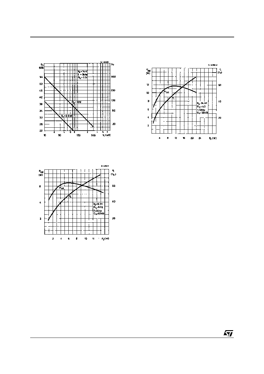
Figure 20 : Gain versus Input Sensitivity
(Stereo amplifier)
Figure 21 : Total Power Dissipation and Effi-
ciency versus Output Power
(Bridge amplifier)
Figure 22 : Total Power Dissipation and Effi-
ciency versus Output Power
(Stereo amplifier)
TDA2005
10/20

Comp.
Recom.
Value
Purpose
Larger Than
Smaller Than
R
1
120 k
Optimization of the Output
Symmetry
Smaller P
o max
Smaller P
o max
R
2
1k
R
3
2 k
R
4
, R
5
12
Closed Loop Gain Setting (see
Bridge Amplifier Design) (*)
R
6
, R
7
1
Frequency Stability
Danger of Oscillation at High
Frequency with Inductive Loads
C
1
2.2
µ
F
Input DC Decoupling
C
2
2.2
µ
F
Optimization of Turn on Pop and
Turn on Delay
High Turn on Delay
Higher Turn on Pop, Higher
Low Frequency Cut-off,
Increase of Noise
C
3
0.1
µ
F
Supply by Pass
Danger of Oscillation
C
4
10
µ
F
Ripple Rejection
Increase of SVR, Increase of
the Switch-on Time
Degradation of SVR.
C
5
, C
7
100
µ
F
Bootstrapping
Increase of Distortion
at low Frequency
C
6
, C
8
220
µ
F
Feedback Input DC Decoupling,
Low Frequency Cut-off
Higher Low Frequency
Cut-off
C
9
, C
10
0.1
µ
F
Frequency Stability
Danger of Oscillation
(*) The closed loop gain must be higher than 32dB.
APPLICATION SUGGESTION
The recommended values of the components are those shown on Bridge applicatiion circuit of Figure 1.
Different values can be used ; the following table can help the designer.
TDA2005
11/20

Figure 23 : Bridge Amplifier without Boostrap
Figure 24 : P.C. Board and Components Layout of Figure 23 (1:1 scale)
APPLICATION INFORMATION
TDA2005
12/20

Figure 25 : Low Cost Bridge Amplifier (G
V
= 42dB)
Figure 26 : P.C. Board and Components Layout of Figure 25 (1:1 scale)
APPLICATION INFORMATION (continued)
TDA2005
13/20

Figure 27 : 10 + 10 W Stereo Amplifier with Tone Balance and LoudnessControl
Figure 28 : Tone Control Response
(circuit of Figure 29)
APPLICATION INFORMATION (continued)
TDA2005
14/20

Figure 29 : 20W Bus Amplifier
Figure 30 : Simple 20W Two Way Amplifier (F
C
= 2kHz)
APPLICATION INFORMATION (continued)
TDA2005
15/20

Figure 31 : Bridge Amplifier Circuit suited for Low-gain Applications (G
V
= 34dB)
Figure 32 : Example of Muting Circuit
APPLICATION INFORMATION (continued)
TDA2005
16/20

BUILT-IN PROTECTION SYSTEMS
Load Dump Voltage Surge
The TDA2005 has a circuit which enables it to
withstanda voltagepulse train, on Pin 9, of the type
shown in Figure 34.
If the supply voltage peaks to more than 40V, then
an LC filter must be inserted between the supply
and pin 9, in order to assure that the pulses at pin
9 will be held withing the limits shown.
A suggestedLC networkis shownin Figure33.With
this network, a train of pulses with amplitude up to
120V and width of 2ms can be applied at point A.
This type of protection is ON when the supply
voltage (pulse or DC) exceeds 18V. For this reason
the maximum operating supply voltage is 18V.
Figure 33
Figure 34
Short Circuit (AC and DC conditions)
The TDA2005 can withstanda permanentshort-cir-
cuit on the output for a supply voltage up to 16V.
Polarity Inversion
High current (up to 10A) can be handled by the
device with no damage for a longer period than the
blow-out time of a quick 2A fuse (normally con-
nected in series with the supply). This feature is
added to avoid destruction, if during fitting to the
car, a mistake on the connection of the supply is
made.
Open Ground
When the ratio is in the ON condition and the
ground is accidentally opened, a standard audio
amplifier will be damaged.On the TDA2005 protec-
tion diodes are included to avoid any damage.
Inductive Load
A protection diode is provided to allow use of the
TDA2005 with inductive loads.
DC Voltage
The maximum operating DC voltage for the
TDA2005 is 18V.
However the device can withstand a DC voltage up
to 28V with no damage. This could occur during
winter if twobatteries are series connectedto crank
the engine.
Thermal Shut-down
The presence of a thermal limiting circuit offers the
following advantages :
1) an overload on the output (even if it is
p er m an e n t ) , o r a n ex c es si ve a mb i en t
temperature can be easily withstood.
2) the heatsink can have a smaller factor of safety
compared with that of a conventional circuit.
There is no device damage in the case of
excessive junction temperature : all that
happens is that P
O
(and thereforeP
tot
) and I
d
are
reduced.
The maximum allowable power dissipation de-
pends upon the size of the external heatsink(i.e. its
thermal resistance) ; Figure 35 shows the dissipa-
ble power as a function of ambient temperature for
different thermal resistance.
Loudspeaker Protection
The circuit offers loudspeaker protection during
short circuit for one wire to ground.
TDA2005
17/20

Figure 35 : Maximum Allowable Power Dissipa-
tion versus Ambient Temperature
Figure 36 : Output Power and Drain Current ver-
sus Case Temperature
Figure 37 : Output Power and Drain Current ver-
sus Case Temperature
TDA2005
18/20

Multiwatt11 V
DIM.
mm
inch
MIN.
TYP.
MAX.
MIN.
TYP.
MAX.
A
5
0.197
B
2.65
0.104
C
1.6
0.063
D
1
0.039
E
0.49
0.55
0.019
0.022
F
0.88
0.95
0.035
0.037
G
1.45
1.7
1.95
0.057
0.067
0.077
G1
16.75
17
17.25
0.659
0.669
0.679
H1
19.6
0.772
H2
20.2
0.795
L
21.9
22.2
22.5
0.862
0.874
0.886
L1
21.7
22.1
22.5
0.854
0.87
0.886
L2
17.4
18.1
0.685
0.713
L3
17.25
17.5
17.75
0.679
0.689
0.699
L4
10.3
10.7
10.9
0.406
0.421
0.429
L7
2.65
2.9
0.104
0.114
M
4.25
4.55
4.85
0.167
0.179
0.191
M1
4.73
5.08
5.43
0.186
0.200
0.214
S
1.9
2.6
0.075
0.102
S1
1.9
2.6
0.075
0.102
Dia1
3.65
3.85
0.144
0.152
OUTLINE AND
MECHANICAL DATA
TDA2005
19/20

Information furnished is believed to be accurate and reliable. However, STMicroelectronics assumes no responsibility for the consequences of
use of such information nor for any infringement of patents or other rights of third parties which may result from its use. No license is granted
by implication or otherwise under any patent or patent rights of STMicroelectronics. Specification mentioned in this publication are subject to
change without notice. This publication supersedes and replaces all information previously supplied. STMicroelectronics products are not
authorized for use as critical components in life support devices or systems without express written approval of STMicroelectronics.
The ST logo is a registered trademark of STMicroelectronics
©
1998 STMicroelectronics ≠ Printed in Italy ≠ All Rights Reserved
STMicroelectronics GROUP OF COMPANIES
Australia - Brazil - Canada - China - France - Germany - Italy - Japan - Korea - Malaysia - Malta - Mexico - Morocco - The Netherlands -
Singapore - Spain - Sweden - Switzerland - Taiwan - Thailand - United Kingdom - U.S.A.
http://www.st.com
TDA2005
20/20