 | –≠–ª–µ–∫—Ç—Ä–æ–Ω–Ω—ã–π –∫–æ–º–ø–æ–Ω–µ–Ω—Ç: TDA2822D | –°–∫–∞—á–∞—Ç—å:  PDF PDF  ZIP ZIP |

TDA2822D
DUAL LOW-VOLTAGE POWER AMPLIFIER
SUPPLY VOLTAGE DOWN TO 1.8V
LOWCROSSOVER DISTORTION
LOW QUIESCENT CURRENT
BRIDGE OR STEREO CONFIGURATION
DESCRIPTION
The TDA2822D is a monolithic integrated circuit
in 8 lead (SO-8) package. It is intended for use as
dual audio power amplifier in portable cassette
players, radios and CD players
September 2003
Æ
APPLICATION CIRCUIT
SO8
ORDERING NUMBER: TDA2822D
ABSOLUTE MAXIMUM RATINGS
Symbol
Parameter
Value
Unit
V
S
Supply Voltage
15
V
I
O
Peak Output
1
A
P
tot
Total Power Dissipation T
amb
= 50
∞
C
0.5
W
T
stg
, T
j
Storage and Junction Temperature
-40 to 150
∞
C
1/6

THERMAL DATA
Symbol
Description
Value
Unit
R
th j-amb
Thermal Resistance Junction-ambient
Max
200
∞
C/W
PIN CONNECTION (Top view)
Figure 1: Stereo Application and Test Circuit
Figure 2: Bridge Application and Test Circuit
TDA2822D
2/6

ELECTRICAL CHARACTERISTICS (V
S
= 6V; T
amb
= 25∞C, unless otherwise specified.
STEREO (Test circuit of fig. 1).
Symbol
Parameter
Test Condition
Min.
Typ.
Max.
Unit
V
S
Supply Voltage
1.8
15
V
I
d
Total Quiescent Drain Current
15
mA
V
O
Quiescent Output Voltage
2.7
V
V
S
= 3V
1.2
V
I
b
Input Bias Current
100
nA
P
O
Output Power (each channel)
(f = 1KHz, d = 10%)
V
S
= 9V
V
S
= 6V
R
L
= 32
V
S
= 4.5V
V
S
= 3V
V
S
= 2V
300
120
60
20
5
mW
R
L
= 16
V
S
= 6V
170
220
mW
R
L
= 8
V
S
= 6V
300
380
mW
R
L
= 4
V
S
= 4.5V
V
S
= 3V
320
110
mW
mW
d
Distortion
R
L
= 32
P
O
= 40mW
0.2
%
R
L
= 16
P
O
= 75mW
0.2
%
R
L
= 8
P
O
= 150mW
0.2
%
G
V
Closed Loop Voltage Gain
f = 1KHz
36
39
41
dB
G
V
Channel Balance
±
1
dB
R
i
Input Resistance
f = 1KHz
100
K
e
N
Total Input Noise
R
s
= 10k
B = Curve A
2
µ
V
R
s
= 10k
B = 22Hz to 22KHz
2.5
µ
V
SVR
Supply Voltage Rejection
f = 100Hz C1 = C2 = 100
µ
F
24
30
dB
C
s
Channel Separation
f = 1KHz
50
dB
BRIDGE (Test circuit of fig.2)
V
S
Supply Voltage
1.8
15
V
I
d
Total Quiescent Drain Current
R
L
=
15
mA
V
os
Output Offset Voltage (between
the outputs)
R
L
= 8
±
80
mV
I
b
Input Bias Current
100
nA
P
O
Output Power
(f = 1KHz, d = 10%)
V
S
= 9V
V
S
= 6V
R
L
= 32
V
S
= 4.5V
V
S
= 3V
V
S
= 2V
320
50
1000
400
200
65
8
mW
R
L
= 16
V
S
= 6V
RL = 16W
V
S
= 3V
800
120
mW
mW
R
L
= 8
V
S
= 4.5V
RL = 8W
V
S
= 3V
700
220
mW
mW
R
L
= 4
V
S
= 3V
RL = 4W
V
S
= 2V
350
80
mW
mW
d
Distortion
R
L
= 8
P
O
= 0.5W f = 1KHz
0.2
%
G
V
Closed Loop Voltage Gain
f = 1KHz
39
dB
R
i
Input Resistance
f = 1KHz
100
K
e
N
Total Input Noise
R
s
= 10k
B = Curve A
2.5
µ
V
R
s
= 10k
B = 22Hz to 22KHz
3
µ
V
SVR
Supply Voltage Rejection
f = 100Hz
40
dB
B
Power Bandwidth (-3dB)
R
L
= 8
P
O
= 1W
120
KHz
TDA2822D
3/6
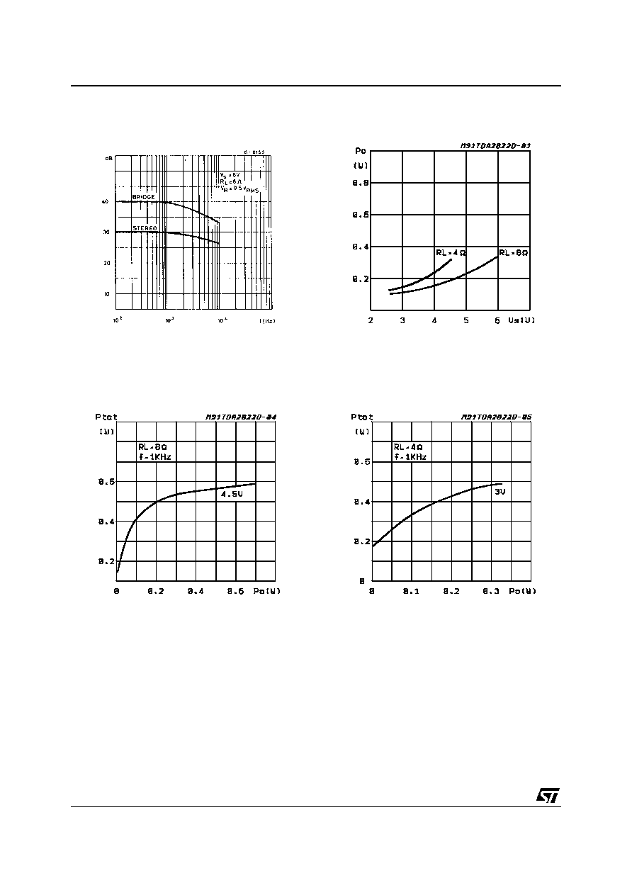
Figure 3: Supply Voltage Rejection vs. Fre-
quency
Figure 4: Output Power vs. Supply Voltage (THD
= 10%, f = 1KHz Stereo)
Figure 5: Total Power Dissipation vs. Output
Power (Bridge)
Figure 6: Total Power Dissipation vs. Output
Power (Bridge)
TDA2822D
4/6

DIM.
mm
inch
MIN.
TYP.
MAX.
MIN.
TYP.
MAX.
A
1.75
0.069
a1
0.1
0.25
0.004
0.010
a2
1.65
0.065
a3
0.65
0.85
0.026
0.033
b
0.35
0.48
0.014
0.019
b1
0.19
0.25
0.007
0.010
C
0.25
0.5
0.010
0.020
c1
45
∞
(typ.)
D (1)
4.8
5.0
0.189
0.197
E
5.8
6.2
0.228
0.244
e
1.27
0.050
e3
3.81
0.150
F (1)
3.8
4.0
0.15
0.157
L
0.4
1.27
0.016
0.050
M
0.6
0.024
S
8
∞
(max.)
(1) D and F do not include mold flash or protrusions. Mold flash or
potrusions shall not exceed 0.15mm (.006inch).
SO8
OUTLINE AND
MECHANICAL DATA
TDA2822D
5/6

Information furnished is believed to be accurate and reliable. However, STMicroelectronics assumes no responsibility for the consequences
of use of such information nor for any infringement of patents or other rights of third parties which may result from its use. No license is
granted by implication or otherwise under any patent or patent rights of STMicroelectronics. Specifications mentioned in this publication are
subject to change without notice. This publication supersedes and replaces all information previously supplied. STMicroelectronics products
are not authorized for use as critical components in life support devices or systems without express written approval of STMicroelectronics.
The ST logo is a registered trademark of STMicroelectronics.
All other names are the property of their respective owners
© 2003 STMicroelectronics - All rights reserved
STMicroelectronics GROUP OF COMPANIES
Australia ≠ Belgium - Brazil - Canada - China ≠ Czech Republic - Finland - France - Germany - Hong Kong - India - Israel - Italy - Japan -
Malaysia - Malta - Morocco - Singapore - Spain - Sweden - Switzerland - United Kingdom - United States
www.st.com
TDA2822D
6/6