TDA3190
COMPLETE TV SOUND CHANNEL
December 1992
1
2
3
4
5
6
7
8
16
15
14
13
12
11
10
9
IF INPUT
IF DECOUPLING
GROUND
FM DETECTOR
DC VOLUME CONTROL
IF DECOUPLING
GROUND
FM DETECTOR
DE-EMPHASIS
RIPPLE REJECTION
SUPPLY VOLTAGE
GROUND
AF OUTPUT
COMPENSATION
AF FEEDBACK
GROUND
3190-01.EPS
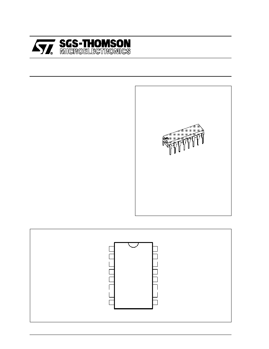
PIN CONNECTIONS
DIP16
(Plastic Package)
ORDER CODE : TDA3190
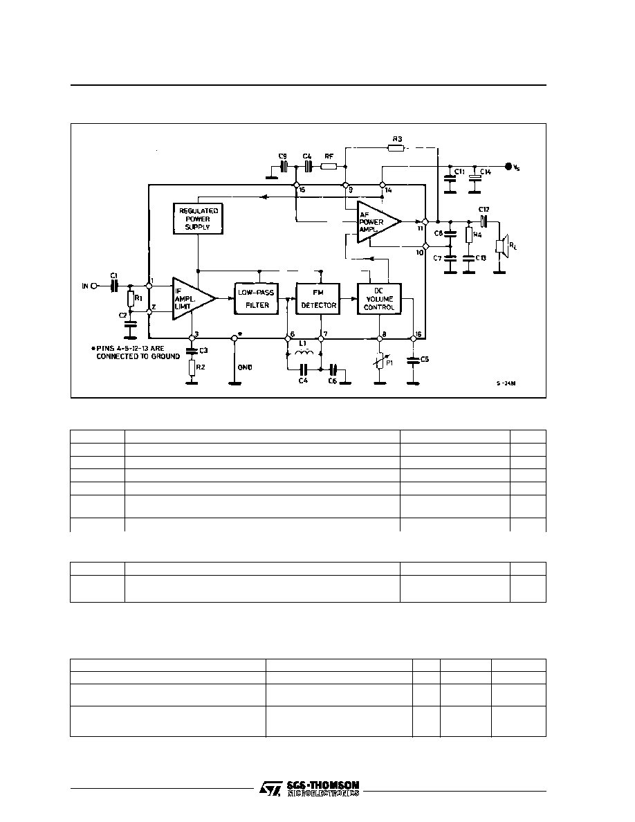
The TDA3190 is a monolithic integrated circuit in a
16-lead dual in-line plastic package. It performs all
the functions needed for the TV sound channel :
.
IF LIMITER AMPLIFIER
.
ACTIVE LOW-PASS FILTER
.
FM DETECTOR
.
DC VOLUME CONTROL
.
AF PREAMPLIFIER
.
AF OUTPUT STAGE
DESCRIPTION
The TDA3190 can give an output power of 4.2 W
(d = 10 %) into a 16
load at V
S
= 24 V, or 1.5 W
(d = 10 %) into an 8
load at V
S
= 12 V. This
performance, together with the FM-IF section char-
acteristics of high sensitivity, high AM rejection and
low distortion, enables the device to be used in
almost every type of television receivers.
The device has no irradiation problems, hence no
external screening is needed.
The TDA3190 is a pin to pin replacement of
TDA1190Z.
1/9
3190-02.EPS
BLOCK DIAGRAM
ABSOLUTE MAXIMUM RATINGS
Symbol
Parameter
Value
Unit
V
S
Supply Voltage (pin 10)
28
V
V
i
Input Signal Voltage (pin 1)
1
V
I
o
Output Peak Current (non-repetitive)
2
A
I
o
Output Peak Current (repetitive)
1.5
A
P
to t
Power Dissipation at T
pins
= 90
�
C
at T
amb
= 70
�
C (free air)
4.3
1
W
W
T
stg
, T
j
Storage and Junction Temperature
� 40 to 150
�
C
3190-01.TBL
THERMAL DATA
Symbol
Parameter
Value
Unit
R
th j-pins
Thermal Resistance Junction-pins
Max
14
�
C/W
R
th j-amb
Thermal Resistance Junction-ambient
Max
80*
�
C/W
* Obtained with the GND pins soldered to printed circuit with minimized copper area.
3190-02.TBL
ELECTRICAL CHARACTERISTICS
(refer to the test circuit, V
S
= 24V, T
amb
= 25
o
C unless otherwise specified)
Symbol
Parameter
Test Conditions
Min.
Typ.
Max.
Unit
V
s
Supply Voltage (Pin 14)
9
28
V
V
o
Quiescent Output Voltage (Pin11)
V
s
= 24V
V
s
= 12V
11
5.1
12
6
13
6.9
V
V
I
d
Quiescent Drain Current
P
1
= 22k
V
s
= 24V
V
s
= 12V
11
22
19
45
40
mA
mA
3190-03.TBL
TDA3190
2/9

ELECTRICAL CHARACTERISTICS
(refer to the test circuit, V
S
= 24V, T
amb
= 25
o
C unless otherwise specified)
Symbol
Parameter
Test Conditions
Min.
Typ.
Max.
Unit
Po
Output Power
d = 10%, f
m
= 400Hz,
f
o
= 4.5MHz,
f =
�
25kHz
V
s
= 24V, R
L
= 16
V
s
= 12V, R
L
= 8
4.2
1.5
W
W
d = 2%, f
m
= 400Hz,
f
o
= 4.5MHz,
f =
�
25kHz
V
s
= 24V, R
L
= 16
V
s
= 12V, R
L
= 8
3.5
1.4
W
W
V
i
Input Limiting Voltage (�3dB)
atPin 1
f
o
= 4.5MHz,
f =
�
7.5kHz,
f
m
= 400Hz, P
1
= 0
40
100
�
V
d
Distortion
P
o
= 50mW, f
m
= 400Hz,
f
o
= 4.5MHz,
f =
�
7.5kHz
V
s
= 24V, R
L
= 16
V
s
= 12V, R
L
= 8
0.75
1
%
%
B
Frequency Response of audio
amplifier (�3dB)
R
L
= 16
, C
8
= 120pF
C
7
= 470pF, P
1
= 22k
R
f
= 82
R
f
= 47
70 to 1200
70 to 7000
Hz
Hz
V
o
Recovered Audio Voltage (Pin16)
V
i
1mV, f
o
= 4.5MHz
f
m
= 400Hz,
f =
�
7.5kHz, P
1
= 0
120
mV
AMR
Ampliture Modulation Rejection
V
i
1mV, f
o
= 4.5MHz,
f
m
= 400Hz,
f
=
�
25kHz, m = 0.3
55
dB
S
+
N
N
Signal to Noise Ratio
V
I
1mV, V
o
= 4V, f
o
= 4.5MHz,
f
m
= 400Hz,
f =
�
25kHz
50
65
dB
R
3
External Feedback Resistance
(betweenPins9and11)
25
k
R
i
Input Resistance (Pin1)
V
i
= 1mV, fo = 4.5MHz
30
k
C
i
Input Capacitance (Pin1)
5
pF
SVR
Supply Voltage Rejection
R
L
= 16
, f
ripple
= 120Hz,
P
1
= 22k
46
dB
A
v
DC Volume Control Attenuation
P
1
= 12k
90
dB
3190-04.TBL
3190-03.EPS
TYPICAL CIRCUIT
TDA3190
3/9

3190-04.EPS
Figure 1 :
Relative Audio Output Voltage and Out-
put Noise versus Input Signal
3190-05.EPS
Figure 2 :
Output Voltage Attenuation versus
DC Volume Control Resistance
3190-06.EPS
Figure 3 :
Amplitude Modulation Rejection
versus Input Signal
3190-07.EPS
Figure 4 :
AMR versus Tuning Frequency
Change
3190-09.EPS
Figure 6 :
Distortion versus Output Power
3190-08.EPS
Figure 5 :
Recovered Audio Voltage versus Un-
loaded Q Factor of the Detector Coil
TDA3190
4/9

3190-10.EPS
Figure 7 :
Distortion versus Frequency
Deviation
3190-11.EPS
Figure 8 :
Distortion versus Tuning Frequency
Change
3190-12.EPS
Figure 9 :
Audio Amplifier Frequency Response
3190-13.EPS
Figure 10 : Supply Voltage Ripple Rejection ver-
sus Ripple Frequency
3190-15.EPS
Figure 12 : Output Power versus Supply Voltage
3190-14.EPS
Figure 11 : Supply Voltage Ripple Rejection ver-
sus Volume Control Attenuation
TDA3190
5/9

3190-16.EPS
Figure 13 : Maximum Power Dissipation versus
Supply Voltage (sinewave operation)
3190-17.EPS
Figure 14 : Power Dissipation and Efficiency ver-
sus Output Power
3190-18.EPS
Figure 15 : Quiescent Output Voltage (Pin 11)
versus Supply Voltage
TDA3190
6/9

The electrical characteristics of the TDA3190 re-
main almost constant over the frequency range 4.5
to 6 MHz, therefore it can be used in all television
standards (FM mod.). The TDA3190 has a high
input impedance,so it can work with a ceramic filter
or with a tuned circuit that provide the necessary
input selectivity.
The value of the resistors connected to pin 9,
determine the AC gain of the audio frequency am-
plifier. This enables the desired gain to be selected
in relation to the frequency deviation at which the
output stage of the AF amplifier, must enter into
clipping.
Capacitor C8, connected between pins 10 and 11,
determines the upper cutoff frequency of the audio
bandwidth. To increase the bandwidth the values of
C8 and C7 must be reduced, keeping the ratio
C7/C8 as shown in the table of fig. 16.
The capacitor connecte d between pin 16 and
ground, together with the internal resistor of 10 K
forms the de-emphasis network. The Boucherot
cell eliminates the high frequency oscillations
caused by the inductiveload and the wires connect-
ing the loudspeaker.
APPLICATION INFORMATION
3190-19.EPS
Figure 16 : Typical Application Circuit
3190-20.TIF
Figure 17 : P.C. Board and Component Layout of the Circuit shown in Figure 16 (1 : 1 scale)
TDA3190
7/9
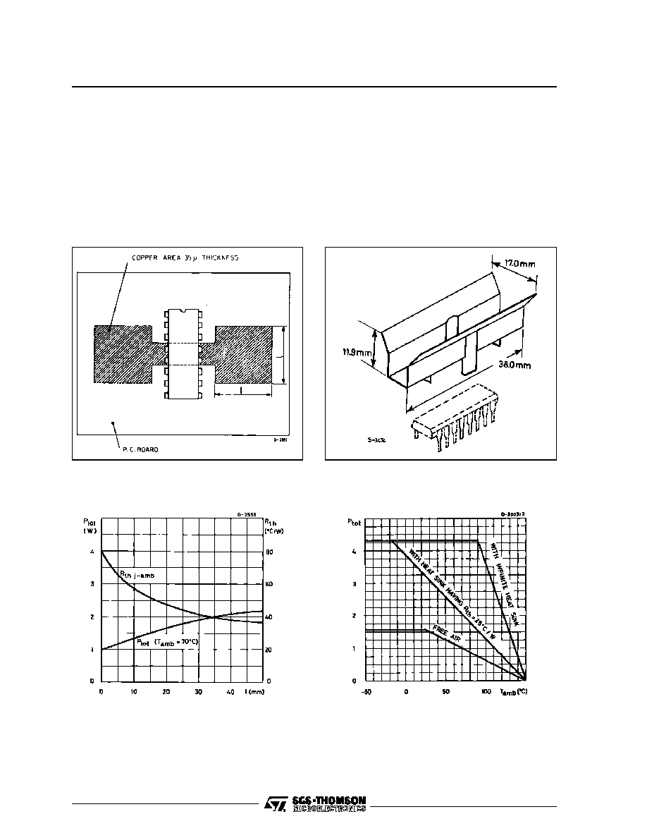
The Rth j-amb of the TDA3190 can be reduced by
soldering the GND pins to a suitable copper area
of the printed circuit board (fig. 18) or to an external
heatsink (fig. 19).
The diagram of figure 20 shows the maximum
dissipable power Ptot and the Rth j-amb as a func-
tion of the side "l" of two equal square copper areas
having a thickness of 35
�
(1.4 mils).
During soldering the pins temperature must not
exceed 260
�
C and the soldering time must not be
longer than 12 seconds.
The external heatsink or printed circuit copper area
must be connected to electrical ground.
MOUNTING INSTRUCTION
3190-21.EPS
Figure 18 : Example of P.C. Board Copper Area
which is used as Heatsink
3190-22.EPS
Figure 19 : External Heatsink Mounting Example
3190-23.EPS
Figure 20 : Maximum Dissipable Power and Junc-
tion to Ambient Thermal Resistance
versus Side "T"
3190-24.EPS
Figure 21 : Maximum Allowable Power Dissipa-
tion versus Ambient Temperature
TDA3190
8/9

16
1
8
I
a1
L
B
e
D
b
Z
e3
F
b1
E
9
PM-DIP16.EPS
PACKAGE MECHANICAL DATA
16 PINS - PLASTIC DIP
Information furnished is believed to be accurate and reliable. However, SGS-THOMSON Microelectronics assumes no responsibility
for the consequences of use of such information nor for any infringement of patents or other rights of third parties which may result
from its use. No licence is granted by implication or otherwise under any patent or patent rights of SGS-THOMSON Microelectronics.
Specifications mentioned in this publication are subject to change without not ice. This publication supersedes and replaces all
information previously supplied. SGS-THOMSON Microelectronics products are not authorized for use as critical components in life
support devices or systems without express written approval of SGS-THOMSON Microelectronics.
�
1994 SGS-THOMSON Microelectronics - All Rights Reserved
Purchase of I
2
C Components of SGS-THOMSON Microelectronics, conveys a license under the Philips
I
2
C Patent. Rights to use these components in a I
2
C system, is granted provided that the system conforms to
the I
2
C Standard Specifications as defined by Philips.
SGS-THOMSON Microelectronics GROUP OF COMPANIES
Australia - Brazil - China - France - Germany - Hong Kong - Italy - Japan - Korea - Malaysia - Malta - Morocco
The Netherlands - Singapore - Spain - Sweden - Switzerland - Taiwan - Thailand - United Kingdom - U.S.A.
Dimensions
Millimeters
Inches
Min.
Typ.
Max.
Min.
Typ.
Max.
a1
0.51
0.020
B
0.77
1.65
0.030
0.065
b
0.5
0.020
b1
0.25
0.010
D
20
0.787
E
8.5
0.335
e
2.54
0.100
e3
17.78
0.700
F
7.1
0.280
i
5.1
0.201
L
3.3
0.130
Z
1.27
0.050
DIP16.TBL
TDA3190
9/9