TDA7250
March 1995
60 W HI-FI DUAL AUDIO DRIVER
.
WIDE SUPPLY VOLTAGE RANGE : 20 TO 90 V
(
±
10 to
±
45 V)
.
VERY LOW DISTORTION
.
AUTOMATIC QUIESCENT CURRENT
CONTROL FOR THE POWER TRANSISTORS
WITHOUT TEMPERATURE SENSE
ELEMENTS
.
OVERLOAD CURRENT PROTECTION FOR
THE POWER TRANSISTORS
.
MUTE/STAND-BY FUNCTIONS
.
LOW POWER CONSUMPTION
.
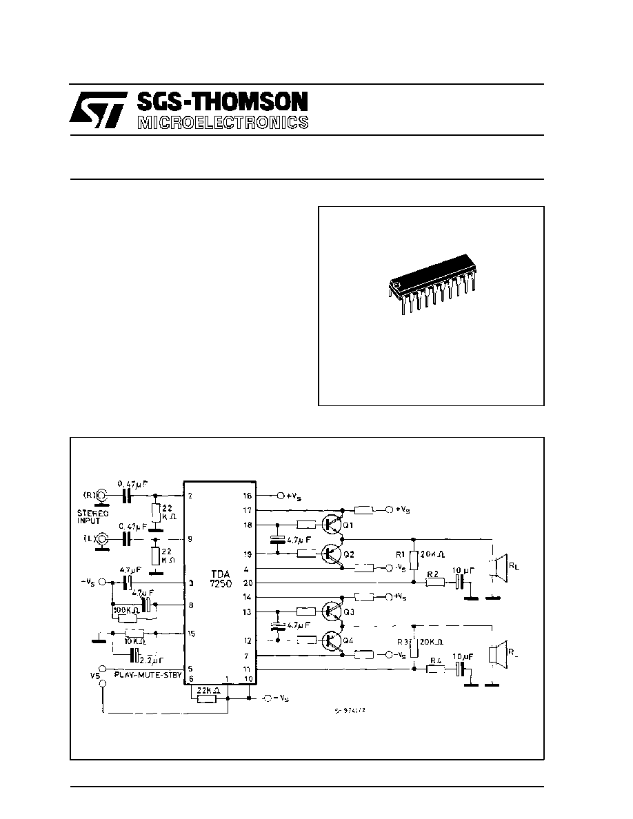
OUTPUT POWER 60 W/8
AND 100 W/4
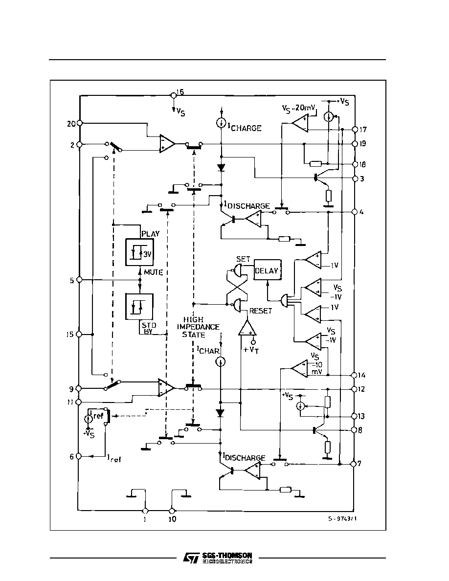
DESCRIPTION
The TDA7250 stereo audio driver is designed to
drive two pair of complementary output transistor in
the Hi-Fi power amplifiers.
DIP20
ORDERING NUMBER : TDA7250
APPLICATION CIRCUIT
1/11
PIN FUNCTIONS
N
∞
Name
Function
1
V
S
≠ POWER SUPPLY
Negative Supply Voltage.
2
NON≠INV. INP. CH. 1
Channel 1 Input Signal.
3
QUIESC. CURRENT
CONTR. CAP. CH1
This capacitor works as an integrator, to control the quiescent current to output
devices in no-signal conditions on channel 1.
4
SENSE (≠) CH. 1
Negative voltage sense input for overload protection and for automatic quiescent
current control.
5
ST. BY / MUTE / PLAY
Three-functions Terminal.
For V
IN
= 1 to 3 V, the device is in MUTE and only quiescent current flows in
the power stages ; - for V
IN
< 1 V, the device is in STAND-BY mode and no
quiescent current is present in the power stages ; - for V
IN
> 3 V, the devic
6
CURRENT PROGRAM
High Impedance Power-stages Monitor.
7
SENSE (≠) CH. 2
Negative Voltage Sense Input for Overload Protection and for Automatic
Quiescent Current Control.
8
QUIESC. CURRENT
CONTR. CAP. CH. 2
This capacitor works as an integrator, to control the quiescent current to output
devices in no-signal conditions on channel 2. If the voltage at its terminals drops
under 250 mV,
it also resets the device from high-impedance state of output
stages.
9
NON≠INV. INP. CH. 2
Channel 2 Input Signals.
10
V
s
≠ POWER SUPPLY
Negative Supply Voltage.
11
INVERT. INP. CH. 2
Feedback from Output (channel 2).
12
OUT (≠) CH. 2
Out Signal to Lower Driver Transistor of Channel 2.
13
OUT (+) CH. 2
Out Signal to Higher Driver Transistor of Channel 2.
14
SENSE (+) CH. 2
Positive Voltage Sense Input for Overload Protection and for Automatic
Quiescent Current Control.
15
COMMON AC GROUND
AC Input Ground in MUTE Condition.
16
V
S
+ POWER SUPPLY
Positive Supply Voltage.
17
SENSE (+) CH. 1
Positive Voltage Sense Input for Overload Protection and for Automatic
Quiescent Current Control.
18
OUT (+) CH. 1
Out Signal to High Driver Transistor of Channel 1.
19
OUT (≠) CH. 1
Out Signal to Low Driver Transistor of Channel 1.
20
INVERT. INP. CH. 1
Feedback from Output (channel 1).
TDA7250
3/11
ELECTRICAL CHARACTERISTICS (T
amb
= 25
∞
C, V
s
=
±
35 V,
play mode,
unless otherwise
specified)
Symbol
Parameter
Test Conditions
Min.
Typ.
Max.
Unit
V
s
Supply Voltage
±
10
±
45
V
I
d
Quiescent Drain Current
Stand-by Mode
8
mA
Play Mode
10
14
I
b
Input Bias Current
0.2
1
µ
A
V
os
Input Offset Voltage
1
±
10
mV
I
os
Input Offset Current
100
200
nA
G
v
Open Loop Voltage Gain
f = 100 Hz
90
dB
f = 10 kHz
60
e
N
Input Noise Voltage
R
G
= 600
B = 20 Hz to 20 kHz
3
µ
V
SR
Slew Rate
10
V/
µ
s
d
Total Harmonic Distortion
G
v
= 26 dB, P
o
= 40 W
f = 1 kHz
f = 20 kHz
0.004
0.03
%
%
V
opp
Output Voltage Swing
60
V
pp
P
o
Output Power (*)
V
s
=
±
35 V, R
L
= 8
V
s
=
±
30 V, R
L
= 8
V
s
=
±
35 V, R
L
= 4
60
40
100
W
W
W
I
o
Output Current
±
5
mA
SVR
Supply Voltage Rejection
f = 100 Hz
75
dB
C
s
Channel Separation
f = 1 kHz
75
dB
MUTE / STANDBY/ PLAY FUNCTIONS
Symbol
Parameter
Test Conditions
Min.
Typ.
Max.
Unit
I
i
Input Current (pin 5)
0.1
µ
A
V
th
Comparator
Standby
/
Mute
Threshold (**)
1.0
1.25
1.5
V
H
Hysteresis Standby / Mute
200
mV
V
th
Comparator Mute / Play
Threshold (**)
2.4
3.0
3.6
V
H
Hysteresis Mute / Play
300
mV
Mute Attenuation
f = 1 kHz
60
dB
V
i
Input Voltage Max. (pin 5)
12 (**)
V
CURRENT SURVEY CIRCUITRY
Symbol
Parameter
Test Conditions
Min.
Typ.
Max.
Unit
Comparator Reference
to + V
S
to ≠ V
S
0.8
0.8
1
1
1.4
1.4
V
V
t
d
Delay Time
10
µ
s
(*) Appli cation circuit of fig. 1
f = 1 KHz ;
d = 0.1 % ;
G
v
= 26 dB.
(**) Referred to
-
V
s
.
QUIESCENT CURRENT CONTROL
Symbol
Parameter
Test Conditions
Min.
Typ.
Max.
Unit
Capacitor Current
Charge
Discharge
30
250
60
500
µ
A
µ
A
Comparator Reference
to + V
S
to ≠ V
S
10
20
10
25
mV
mV
TDA7250
5/11