 | ÐлекÑÑоннÑй компоненÑ: TDA7269SA | СкаÑаÑÑ:  PDF PDF  ZIP ZIP |
Äîêóìåíòàöèÿ è îïèñàíèÿ www.docs.chipfind.ru
1/11
TDA7269SA
September 2004
1
FEATURES
WIDE SUPPLY VOLTAGE RANGE UP TO
+20V
SPLIT SUPPLY
10+10W @THD = 10%, R
L
= 8
, V
S
=
±
14V
NO POP AT TURN-ON/OFF
MUTE (POP FREE)
STAND-BY FEATURE (LOW I
q
)
SHORT CIRCUIT PROTECTION TO GND
THERMAL OVERLOAD PROTECTION
CLIPWATT 11 PACKAGE
2
DESCRIPTION
The TDA7269SA is class AB power amplifier assem-
bled in the @ Clipwatt 11 package, specially de-
signed for high quality sound application as Hi-Fi
music centers and stereo TV sets.
The TDA7269SA is pin to pin compatible with
TDA7269, TDA7269A, TDA7269ASA, TDA7265,
TDA7499, TDA7499SA.
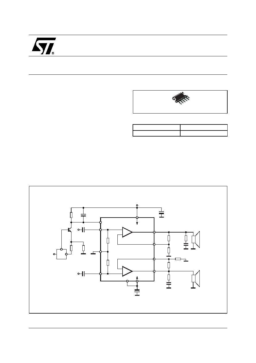
10W+10W STEREO AMPLIFIER WITH MUTE & ST-BY
Figure 2. Block Diagram
+5V
18K
15K
IN (L)
1
µ
F
15K
1
µ
F
MUTE/
ST-BY
GND
IN (R)
1
µ
F
4.7
4.7
100nF
100nF
OUT (L)
OUT (R)
1000
µ
F
1000
µ
F
+V
S
3
5
7
9
6
11
2
4
+
+
-
-
D94AU085
RL (L)
RL (R)
-V
S
µ
P
560
18K
IN- (L)
8
10
IN- (R)
1
560
18K
Rev. 2
Figure 1. Package
Table 1. Order Codes
Part Number
Package
TDA7269SA
Clipwatt11
Clipwatt11
TDA7269SA
2/11
Table 2. Absolute Maximum Ratings
Figure 3. Pin Connection (Top view)
Table 3. Thermal Data
Figure 4. Single Supply Application
Symbol
Parameter
Value
Unit
V
S
DC Supply Voltage
±22
V
I
O
Output Power Current (internally limited)
3
A
P
tot
Total Power Dissipation (Tamb = 70°C)
20
W
T
amb
Ambient Operating Temperature (1)
0 to 70
°C
T
stg
, T
j
Storage and Junction Temperature
-40 to 150
°C
Symbol
Parameter
Value
Unit
R
th j-case
Thermal Resistance Junction-case Max.
3.9
°C/W
R
th j-amb
Thermal Resistance Junction-ambient
48
°C/W
1
2
3
4
5
6
7
9
10
11
8
IN+(1)
IN-(1)
GND
IN-(2)
IN+(2)
-V
S
MUTE
OUTPUT(2)
+V
S
OUTPUT(1)
-V
S
D03AU1506
PLAY
5V
R2
15K
IN (L)
C3 1
µ
F
R1
10K
C1
1
µ
F
MUTE
IN (R)
C4 1
µ
F
R8
4.7
R7
1K
C7
0.1
µ
F
OUT (L)
OUT (R)
C5
1000
µ
F
+V
S
3
5
7
9
6
11
2
4
+
+
-
-
D96AU444A
OUT
(L)
OUT
(R)
GND
R4
30K
IN- (L)
8
10
IN- (R)
1
R5
1K
R6
30K
R9
4.7
C9 470
µ
F
C10 470
µ
F
C8
0.1
µ
F
R3
15K
0
MUTE
Q1
BSX33
C6
0.1
µ
F
D1 5.1V
C2
100
µ
F
3/11
TDA7269SA
Table 4. ELECTRICAL CHARACTERISTCS
(Refer to the test circuit V
S
= ±14V; R
L
= 8
; R
S
= 50
;
G
V
= 30dB, f = 1KHz; T
amb
= 25°C, unless otherwise
specified)
(*) In mute condition the current drawn from Pin 5 must be
650
µ
A
Symbol
Parameter
Test Condition
Min.
Typ.
Max.
Unit
V
S
Supply Voltage Range
R
L
= 8
;
R
L
= 4
;
±5
±5
±20
±15
V
V
I
q
Total Quiescent Current
60
100
mA
V
OS
Input Offset Voltage
-25
25
mV
I
b
Non Inverting Input Bias Current
500
nA
P
O
Output Power
THD = 10%;
R
L
= 8
;
V
S
= ±12.5V; R
L
= 4
;
8
7.5
10
10
W
W
THD = 1%;
R
L
= 8
;
V
S
= ±12.5V; R
L
= 4
;
7.5
7.5
W
W
THD
Total Harmonic Distortion
R
L
= 8
; P
O
= 1W; f = 1KHz;
0.03
%
R
L
= 8
; P
O
= 0.1 to 5W;
f = 100Hz to 15KHz;
0.7
%
R
L
= 4
; P
O
= 1W; f = 1KHz;
0.02
%
R
L
= 4
; V
S
= ±10V;
P
O
= 0.1 to 5W;
f = 100Hz to 15KHz;
1
%
C
T
Cross Talk
f = 1KHz;
f = 10KHz;
50
70
60
dB
dB
SR
Slew Rate
6.5
10
V/
µ
s
G
OL
Open Loop Voltage Gain
80
dB
e
N
Total Output Noise
A Curve
f = 20Hz to 22KHz
3
4
8
µ
V
µ
V
R
i
Input Resistance
15
20
K
SVR
Supply Voltage Rejection
(each channel)
f = 100Hz; V
R
= 0.5V
60
dB
T
j
Thermal Shut-down Junction
Temperature
145
°C
MUTE FUNCTION [ref +V
S
] (*)
V
MUTE
Mute /Play threshold
-7
-6
-5
V
A
MUTE
Mute Attenuation
60
70
dB
STAND-BY FUNCTIONS [ref: +V
S
] (only for Split Supply)
V
ST-BY
Stand-by Mute threshold
-3.5
-2.5
-1.5
V
A
ST-BY
Stand-by Attenuation
110
dB
I
qST-BY
Quiescent Current @ Stand-by
3
6
mA
TDA7269SA
4/11
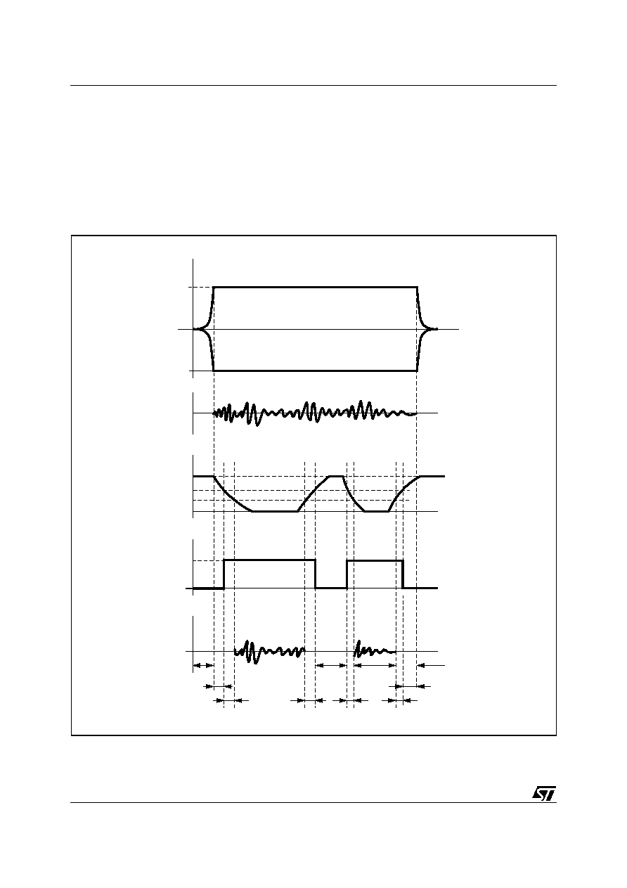
3
MUTE STAND-BY FUNCTION
The pin 5 (MUTE/STAND-BY) controls the amplifier status by two different thresholds, referred to +V
S
.
When V
pin5
higher than = +V
S
-2.5V the amplifier is in Stand-by mode and the final stage generators
are off.
When V
pin5
between = +V
S
-2.5V and V
S
-6V the final stage current generators are switched on and
the amplifier is in mute mode.
When V
pin5
lower than = +V
S
-6V the amplifier is play mode.
Figure 5.
t
OFF
STDBY
MUTE
MUTE
MUTE
MUTE
PLAY
STDBY
PLAY
OFF
STDBY
20
+V
S
(V)
-20
-V
S
V
IN
(mV)
Vpin5
(V)
V
S
V
S
-2.5
V
S-
6
V
S
-10
I
q
(mA)
0
VOUT
(V)
D94AU086
5/11
TDA7269SA
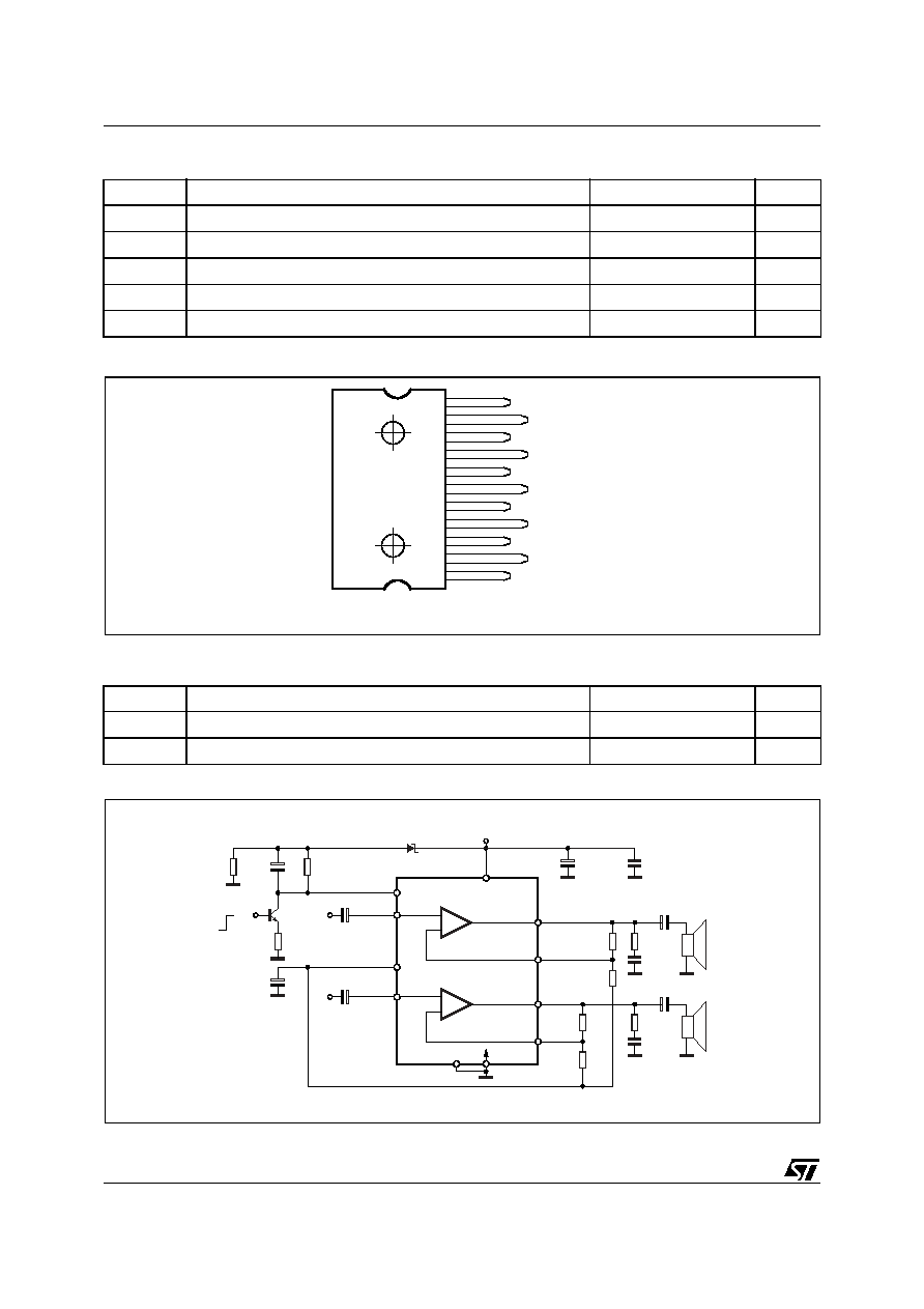
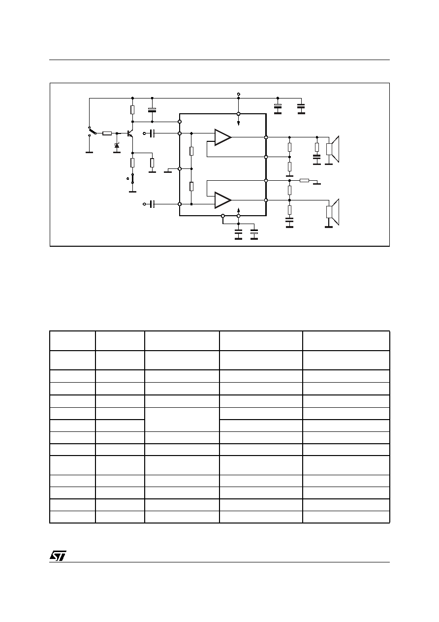
Figure 6. Test and Application Circuit (Stereo Configuration)
4
APPLICATION SUGGESTIONS
4.1 (Demo Board Schematic)
The recommended values of the external components are those shown the demoboard schematic different val-
ues can be used, the following table can help the designer
Table 5. .
(*) Closed loop gain has to be
25dB
COMPONENT
SUGGESTION
VALUE
PURPOSE
LARGER THAN
RECOMMENDED VALUE
SMALLER THAN
RECOMMENDED VALUE
R1
10K
Mute Circuit
Increase of Dz Biasing
Current
R2
15K
Mute Circuit
V
pin
#5 Shifted Downward
V
pin
#5 Shifted Upward
R3
18K
Mute Circuit
V
pin
#5 Shifted Upward
V
pin
#5 Shifted Downward
R4
15K
Mute Circuit
V
pin
#5 Shifted Upward
V
pin
#5 Shifted Downward
R5, R8
18K
Closed Loop Gain
Setting (*)
Increase of Gain
R6, R9
560
Decrease of Gain
R7, R10
4.7
Frequency Stability
Danger of Oscillations
Danger of Oscillations
C1, C2
1
µ
F
Input DC Decoupling
Higher Low Frequency Cutoff
C3
1
µ
F
St-By/Mute Time
Constant
Larger On/Off Time
Smaller On/Off Time
C4, C6
1000
µ
F
Supply Voltage Bypass
Danger of Oscillations
C5, C7
0.1
µ
F
Supply Voltage Bypass
Danger of Oscillations
C8, C9
0.1
µ
F
Frequency Stability
Dz
5.1V
Mute Circuit
R3
IN (L)
C1
R2
C3
MUTE/
ST-BY
GND
IN (R)
C2
R7
R10
C8
C9
OUT (L)
OUT (R)
C6
C4
+V
S
3
5
7
9
6
11
2
4
+
+
-
-
D94AU087B
RL (L)
RL (R)
+V
S
-V
S
R9
R5
IN- (L)
8
10
IN- (R)
1
SW1
R1
DZ
R4
SW2
C7
R8
R6
C5
Q1
ST-BY
MUTE
Document Outline