 | –≠–ª–µ–∫—Ç—Ä–æ–Ω–Ω—ã–π –∫–æ–º–ø–æ–Ω–µ–Ω—Ç: TDA7278 | –°–∫–∞—á–∞—Ç—å:  PDF PDF  ZIP ZIP |
TDA7278
HIGH-EFFICIENCY CD ACTUATOR DRIVER
WIDE OPERATIVE SUPPLY RANGE (1.6 to
5V) LOW VOLTAGE OPERATION CAPABIL-
ITY
4 LOAD DRIVING VOLTAGES PWM REGU-
LATED (STEP DOWN FROM BATTERY)
LOW ON RESISTANCE H BRIDGES
(2 x 1.6
MAX + 2 x 2.5
MAX) FOR:
≠ FOCUS AND TRACKING ACTUATORS
≠ SLEDGE AND SPINDLE MOTORS
SYNCHRONIZABLE SAWTOOTH OSCILLATOR
CONFIGURABLE DC/DC CONVERTER FOR
ADJUSTABLE MAIN POWER SUPPLY, WITH
LOW ON RESISTANCE (0.4
MAX) SWITCH
GENERAL ENABLE INPUT
ADJUSTABLE WATCH DOG AND DELAYED
POWER ON RESET FUNCTIONS
ADJUSTABLE COMPARATORS FOR BAT-
TERY LOW AND BATTERY EMPTY DETEC-
TION
March 1997
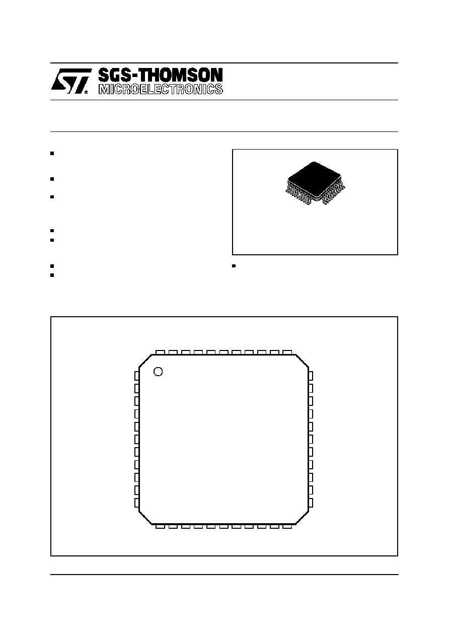
PQFP44
1
2
3
5
6
4
7
8
9
10
17
11
18
19
20
21
22
44
43
42
41
39
40
38
37
36
35
34
28
27
26
24
23
25
33
32
31
29
30
GND
FLIN 1
VBAT
H OUT 2A
H IN 2
FLIN 2
VHIGH
OUT
H OUT 1B
H OUT 1A
H IN 1
SSCAP
INP
IRC
VCPU
OUT2
OUT1
VBG
RESET
CRES
WDINP
STCAP
H
OUT
2B
ERROR
1
ERROR
2
BEMP
VCON
BLOW
VREF(2)
VREF(1)
ERROR
4
ERROR
3
H
OUT
4B
GND
H OUT 3A
H IN 3
ENABLE
SYNC
H OUT 3B
H IN 4
H OUT 4A
FLIN 4
FLIN 3
VBAT
D94AU112A
12
13
14
15
16
PIN CONNECTION
1/15
ABSOLUTE MAXIMUM RATINGS (25
∞
C)
Pin Name
Min
Max
Unit
HIN 1, HIN 2, HIN 3, HIN 4
-0.4
8
V
HOUT 1A, HOUT 2A, HOUT 3A, HOUT 4A, HOUT 1B, HOUT 2B, HOUT 3B,
HOUT 4B
-0.4
8
V
FLIN 1, FLIN 2, FLIN 3, FLIN 4
-0.4
10
V
ERROR 1, ERROR 2, ERROR 3, ERROR 4,
-0.4
7
V
V
BAT
-0.4
8
V
V
REF 1
, V
REF 2
-0.4
7
V
BLOW, BEMP, V
CON
-0.4
7
V
OUT, VHIGH
-0.4
16
V
OUT 2
-0.4
8
V
OUT 1
-0.4
16
V
SSCAP, IRC, INP
-0.4
7
V
VCPU
-0.4
7
V
VBG, RESET, CRES, WDINP, STCAP, SYNC
-0.4
7
V
EN
-0.4
8
V
* Pin 1, 8, 12, 14, 20, 26 and 33 are ESD sensitive (max. voltage
±
1KV)
THERMAL DATA
Symbol
Parameter
Value
Unit
T
op
Operating Temperature range
≠25 to 70
∞
C
T
j
Max. Junction Temperature
100
∞
C
T
j-amb
Thermal Resistance Junction to Ambient
70
∞
C/W
TDA7278
2/15

PIN FUNCTIONS
N
o
Name
Function
21
WDINP
Watch dog input - AC coupled to WD
µ
controller output
(Disabled when connected to GND)
Watch dog & reset
circuit
20
CRES
Start up reset control for
µ
C & watch dog time constant
19
RESET
Reset output command to
µ
C (open collector)
41
BEMP
Battery empty comparator input
Battery control circuit
40
BLOW
Battery low comparator input
39
VCON
Battery level control output
VCON = Z VBEMP > VBCON > VBG
VCON = 1 VBEMP > VBG > VBLOW
VCON = 0 VBG > VBEMP > VBLOW
24
ENABLE
General Enable Input (active Low)
Band Gap Reference
18
VBG
Reference voltage capacitor
12
SSCAP
Soft start capacitor
VCPU DC-DC
converter
16
OUT 1
Switching transistor terminal high
17
OUT 2
Switching transistor terminal low
15
VCPU
Regulated voltage
14
IRC
Error amplifier output
13
INP
Error amplifier inverting input
11
VHIGH
Regulated Voltage
Vhigh Boost DC-DC
Converter
10
OUT
Switching transistor output
22
STCAP
Sawtooth toth
Oscillator
23
SYNC
Oscillator synchronizing input
4, 30
V
BAT
Power supply voltage
6, 28
GND
Power ground
38
VREF 2
Buffered reference output voltage
37
VREF 1
Reference input voltage
5
FLIN 1
Switching Output
Focus actuator step
down converter
& H bridge
7
HOUT 1A
H bridge positive output
8
HIN 1
Regulated voltage H bridge supply
9
HOUT 1B
H bridge negative output
43
ERROR 1
Error input
29
FLIN 3
Switching Output
Tracking actuator
step down converter
& H bridge
27
HOUT 3A
H bridge positive output
26
HIN 3
Regulated voltage H bridge supply
25
HOUT 3B
H bridge negative output
35
ERROR 3
Error input
3
FLIN 2
Switching output
Spindle motor step
down converter
& H bridge
2
HOUT2A
H bridge positive output
1
HIN 2
Regulated voltage H bridge supply
44
HOUT 2B
H bridge negative output
42
ERROR 2
Error input
TDA7278
3/15

ELECTRICAL CHARACTERISTICS (T
amb
= 25
∞
C, V
BAT
= 1.6V unless otherwise specified)
Symbol
Parameter
Test Condition
Min.
Typ.
Max.
Unit
V
BAT
Power Supply
(T
amb
= 25 to 70
∞
C)
Config. in fig. 3a: V
CPU
<4V
Config. in fig. 3a: V
CPU
>4V
Config. in fig. 3b
Config. in fig. 3c
Stand-by condition
Config. in fig 3a
1.6
1.6
V
CPU
+0.3
1.6
V
CPU
4
4
4
4
V
V
V
V
V
Power Supply
(T
amb
= 25 to 60
∞
C)
Config. in fig. 3a
Config. in fig. 3b
Config. in fig. 3c
Stand-by condition
Config. in fig 3a
1.6
V
CPU
+0.3
1.6
V
CPU
5
5
5.5
V
V
V
V
Current Consumption from
V
CPU
(1)
V
CPU
= 5V
5
mA
Current Consumption from
V
BAT
(3)
1.5
mA
Leakage Current in stand-
by condition
V
BAT
= 5V
20
µ
A
V
HIGH
V
CPU
(adj)
Output Voltages
V
BAT
+4
2.4
V
BAT
+7
V
BAT
+12
5
V
V
R
ON
of DC/DC Converter Switch I = 1A
0.25
0.4
Max Output Current from
V
CPU
V
CPU
< 4.5V Config. fig 3a
150
mA
Voltage Ripple on V
CPU
Oscillator - free freq.
- sync. freq
-
free freq.
STCAP = 470pF
.
V
BAT
= 1.6 to 5V
80
200
180
20
KHz
KHz
KHz
H_bridge
- Ron, actuators (CH 1,3)
- Ron, motors (CH 2,4)
I = 100mA
1.0
1.6
1.6
2.5
PWM Circuit
- Ron, actuators
- Ron, motors
I = 100mA
0.5
0.8
0.8
1.25
V
BG
Reference Voltage
1.22
1.28
1.34
V
Load Regulation
I
LOAD
=-10 to+10
µ
A;
-30
30
mV
Line Regulation
V
BAT
= 1.6 to 5V
30
mV
AV
Bridge gain
From Error to H
IN
2.8
3.6
4.5
K
Reset Time Coefficient
note 2
7.4
11
17.2
msec/
µ
F
Z
IN
Error Impedance Inputs
26
40
k
V
REF2
Load Regulation
I
LOAD
=-1 to+1mA
≠30
30
mV
V
REF1
Impedance
750
k
WINDIP Impedance
30
k
BEMP & BLOW
intervention threshold
0.55
0.65
0.75
V
RESET Voltage Saturation
I
LOAD
=-100
µ
A
200
mV
VCON Voltage Saturation
I
LOAD
=-100
µ
A
I
LOAD
=100
µ
A
V
CPU
-200
200
mV
mV
(1): all the 4 PWM outputs switched off.
(2) T
RESET
= width of the Reset pulse on pin 19 = K
C, where C is the capacitance on pin 20 (C
RES
).
To avoid reset, the frequency of watch dog pulses must be greater than (3
T
RESET
)
-1
(3) All the 4 PWM output switched OFF, auxiliary and main DC/DC converters polarized but not switching
TDA7278
4/15

OSCILL
DRIV
VHIGH
+
-
Vbg
VREF (2)
VHIGH
OUT
SYNC
ST CAP
V bg
ER
+
-
S
R
Q
VBAT
-
+
DRIV
VHIGH
DRIV
VHIGH
FL IN 1
DRIV
VHIGH
ER
+
-
S
R
Q
VBAT
-
+
DRIV
VHIGH
DRIV
VHIGH
DRIV
VHIGH
ER
+
-
S
R
Q
VBAT
-
+
DRIV
VHIGH
DRIV
VHIGH
DRIV
VHIGH
ER
+
-
S
R
Q
VBAT
-
+
DRIV
VHIGH
DRIV
VHIGH
H IN 1
H OUT 1A
H OUT 1B
FL IN 3
H IN 3
H OUT 3A
H OUT 3B
FL IN 2
H IN 2
H OUT 2A
H OUT 2B
FL IN 4
H IN 4
H OUT 4A
H OUT 4B
DRIV
VHIGH
REFERENCE
and
THERMAL
Vbg
Vbg
CONTROL
VCPU
Vbg/2
Vbg/2
-
+
-
+
VCPU
OUT1
OUT2
IRC
INP
SSCAP
VBG
ENABLE
RESET
CRES
WD INP
BEMP
BLOW
VCON
GND
ERROR
2
ERROR
4
VREF
(1)
ERROR
3
ERROR
1
VBAT
D94AU078B
22
38
11
10
23
4
30
37
43
35
13
14
15
16
17
VBAT
12
18
24
19
20
21
41
40
39
6
28
42
36
34
32
33
31
44
2
1
3
25
27
26
29
9
7
8
5
GND
VBAT
Vbg/2
Figure 1: Block Diagram.
TDA7278
5/15