 | –≠–ª–µ–∫—Ç—Ä–æ–Ω–Ω—ã–π –∫–æ–º–ø–æ–Ω–µ–Ω—Ç: TDA7300D | –°–∫–∞—á–∞—Ç—å:  PDF PDF  ZIP ZIP |

TDA7300
DIGITAL CONTROLLED STEREO AUDIO PROCESSOR
SINGLE SUPPLY OPERATION
FOUR STEREO INPUT SOURCE SELEC-
TION
MONO INPUT
TREBLE, BASS, VOLUME, AND BALANCE
CONTROL
FOUR INDEPENDENT SPEAKER CONTROL
(FRONT/REAR)
SINGLE SUPPLY OPERATION
ALL FUNCTIONS PROGRAMMABLE VIA SE-
RIAL BUS
VERY LOW NOISE AND VERY LOW DIS-
TORTION
POP FREE SWITCHING
DESCRIPTION
The TDA7300 is a volume, tone (bass and treble),
balance (left/right) and fader (front/rear) proces-
sor for high quality audio applications in car radio
and Hi-Fi systems.
Control is accomplished by serial bus microproc-
essor interface.
The AC signal setting is obtained by resistor net-
works and analog switches combined with opera-
tional amplifiers.
The results are: low noise, low distortion and high
dynamic range.
This is advanced information on a new product now in development or undergoing evaluation. Details are subject to change without notice.
May 1991
BLOCK DIAGRAM
DIP28
SO28
ORDERING NUMBERS:
TDA7300
TDA7300D
1/16

ABSOLUTE MAXIMUM RATINGS
Symbol
Parameter
Value
Unit
V
S
Supply Voltage (V
S1
)
18
V
T
amb
Operating Ambient Temperature Range
-40 to +85
∞
C
T
stg
Storage Temperature
-40 to 150
∞
C
THERMAL DATA
Symbol
Description
SO28
DIP28
Unit
R
th j-pins
Thermal Resistance Junction-pins
Max
85
65
∞
C/W
ELECTRICAL CHARACTERISTICS (T
amb
= 25
∞
C, V
S1
= 12V or V
S2
= 8.5V , R
L
= 10k
and R
g
= 600
,
f = 1KHz unless otherwise specified)
Symbol
Parameter
Test Condition
Min.
Typ.
Max.
Unit
SUPPLY (1)
V
S1
Supply Voltage VS1
10
12
16
V
V
S2
Supply Voltage VS2
6
8.5
10
V
I
S2
Supply Current
15
30
40
mA
V
ref
Reference Voltage (pin 7)
3.5
4.3
5
V
SVR
Ripple Rejection at V
S1
f = 300Hz to 10KHz
80
97
dB
SVR
Ripple Rejection at V
S2
f = 300Hz to 10KHz
50
58
dB
INPUT SELECTORS
R
i
Input Resistance
30
45
K
V
IN max
Max. Input Signal
GV = 0dB
d = 0.3%
1.5
2.2
Vrms
IN
S
Input Separation
f = 1KHz (2)
90
100
dB
f = 10KHz (2)
70
80
dB
V
i (DC)
Input DC Voltage
3.5
4.3
5
V
PIN CONNECTION (Top view)
TDA7300
2/16

ELECTRICAL CHARACTERISTICS (continued)
Symbol
Parameter
Test Condition
Min.
Typ.
Max.
Unit
VOLUME CONTROLS
Control Range
78
dB
G
max
Max Gain
8
10
12
dB
Max Attenuation
64
68
dB
Step Resolution
G
V
= -50 to 10dB
2
3
dB
Attenuator Set Error
2
dB
Tracking Error
2
dB
SPEAKER ATTENUATORS
Control Range
35
38
41
dB
Step Resolution
2
3
dB
Attenuator Set Error
2
dB
Tracking Error
2
dB
BASS AND TREBLE CONTROL (3)
Control Range
±
15
dB
Step Resolution
2.5
3.5
dB
AUDIO OUTPUT
V
O
Max. Output Voltage
d = 0.3%
1.5
2.2
Vrms
R
L
Output Load Resistance
2
K
C
L
Output Load Capacitance
1
nF
R
O
Output Resistance
70
150
V
O
(DC)
DC Voltage Level
3
3.8
4.5
V
GENERAL
e
NO
Output Noise
BW = 22Hz to 22KHz, G
v
= 0dB
6
15
µ
V
Curve A
G
v
= 0dB
4
S/N
Signal to Noise Ratio
All gain = 0dB V
O
= 1Vrms
BW = 22Hz to 22KHz
105
dB
d
Distortion
f = 1KHz; V
O
= 1V; G
v
= 0
0.01
0.1
%
Frequency Response (-1dB)
G
v
= 0
High
Low
20
20
KHz
Hz
S
C
Channnel Separation left/right
f = 1KHz
f = 10KHz
90
70
100
80
dB
dB
BUS INPUTS
V
IL
Input LOW Voltage
0.8
V
V
IH
Input HIGH Voltage
2.4
V
V
O
Output Voltage SDA Acknowledge
I = 1.6mA
0.4
V
Digital Input Current
-5
+5
µ
A
Notes:
(1) The circuit can be supplied either at V
S1
or without the use of the internal voltage regulator at V
S2
. The circuit also operates at a supply
voltage V
S1
lower than 10V. In this case the ripple rejection of V
S2
is valid, because the voltage regulator saturates to a saturation voltage
of about 0.8V.
(2) The selected input is grounded thru the 2.2
µ
F capacitor.
(3) Bass and Treble response see attached diagram. The center frequency and quality of the resonance behaviour can be choosen by the
external circuitry. A standard first order bass response can be realized by a standard feedback network.
TDA7300
3/16
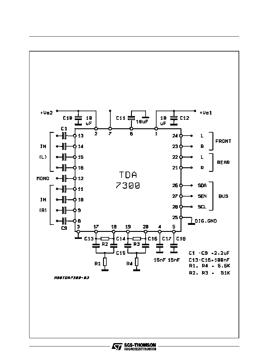
Figure 1: Application Circuit
TDA7300
4/16

Figure 2: P.C. Board and Components Layout of the Fig.1 (1:1 scale)
TDA7300
5/16

Figure 3: Total Output Noise vs. Volume Setting
Figure 5: Distortion + Noise vs. Frequency
Figure 7: Distortion vs. Load Resistance
Figure 4: Signal to Noise Ratio vs. Volume
Setting
Figure 6: Distortion vs. Output Voltage
Figure 8: Channel Separation (L1 - R1) vs.
Frequency
TDA7300
6/16

Figure 9: Input Separation (L1 - L2) vs. (V
S1
)
Frequency
Figure 10: Supply Voltage Rejection (V
S1
) vs.
Frequency
Figure 11: Supply Voltage Rejection (V
S2
) vs.
Frequency
Figure 12: Supply Voltage Rejection vs. V
S1
Figure 13: Supply Voltage Rejection vs. V
S2
Figure 14: Clipping Level (Vrms) vs. Supply
Voltage
TDA7300
7/16

APPLICATION INFORMATION
Volume Control Concept
Traditional electronic volume control circuits use a
multiplier technique with all the disadvantages of
high noise and distortion.
The used concept, as shown in Fig. 15 with digital
switched resistor dividers, provides extremely low
noise and distortion. The multiplexing of the resis-
tive dividers is realized with a multiple-input op-
erational amplifier.
Bass and Treble Control
The principle operation of the bass control is
shown in Fig. 16. The external filter together with
the internal buffer allows a flexible filter design ac-
cording to the different requirements in car radios.
The function of the treble is similar to the bass.
A typical curve is shown in Fig.19.
Outputs
A special class-A output amplifier with a modu-
lated sink current provides low distortion and
ground compatibility with low current consump-
tion.
Figure 15: Volume Control
Figure 16: Bass Control
Figure 17: Quiescent Current vs. Supply Voltage
Figure 18: Quiescent Current vs. Temperature
TDA7300
8/16

APPLICATION INFORMATION (continued)
Figure 19: Typical Tone Response
Figure 20: Complete Car-Radio System using Digital Controlled Audio Processor
TDA7300
9/16

APPLICATION INFORMATION (continued)
SERIAL BUS INTERFACE
S-BUS Interface and I
2
CBUS Compatibility
Data transmission from microprocessor to the
TDA7300 and viceversa takes place thru the 3-
wire S-BUS interface, consisting of the three lines
SDA, SCL, SEN. If SDA and SEN inputs are
short-circuited together, then the TDA7300 ap-
pears as a standard I
2
CBUS slave.
According to I
2
CBUS specification the S-BUS
lines are connected to a positive supply voltage
via pull-up resistors.
Data Validity
As shown in fig. 21, the data on the SDA line
must be stable during the high period of the clock.
The HIGH and LOW state of the data line can
only change when the clock signal on the SCL
line is LOW.
Start and Stop Conditions
I
2
CBUS:
as shown in fig.22 a start condition is a HIGH to
LOW transition of the SDA line while SCL is
HIGH. The stop condition is a LOW to HIGH tran-
sition of the SDA line while SCL is HIGH.
S-bus:
the start/stop conditions (points 1 and 6) are de-
tected exclusively by a transition of the SEN line
(1
0 / 0
1) while the SCL line is at the HIGH
level.
The SDA line is only allowed to change during the
time the SCL line is low (points 2, 3, 4, 5). After
the start information (point 1) the SEN line returns
to the HIGH level and remains unchanged for all
the time the transmission is performed.
Byte Format
Every byte transferred on the SDA line must con-
tain 8 bits. Each byte must be followed by an ac-
knowledge bit. The MSB is transferred first.
Acknowledge
The master (
µ
P) puts a resistive HIGH level on the
SDA line during the acknowledge clock pulse (see
fig. 23). The peripheral (audioprocessor) that ac-
knowledges has to pull-down (LOW) the SDA line
during the acknowledge clock pulse, so that the
SDA line is stable LOW during this clock pulse.
The audioprocessor which has been addressed
has to generate an acknowledge after the recep-
tion of each byte, otherwise the SDA line remains
at the HIGH level during the ninth clock pulse
time. In this case the master transmitter can gen-
erate the STOP information in order to abort the
transfer.
Figure 21: Data Validity on the I
2
CBUS
Figure 22: Timing Diagram of S-BUS and I
2
CBUS
TDA7300
10/16

Transmission without Acknowledge
Avoiding to detect the acknowledge of the audio-
processor, the
µ
P can use a simplier transmission:
simply it waits one clock without checking the slave
acknowledging, and sends the new data.
This approach of course is less protected from
misworking and decreases the noise immunity.
Interface Protocol
The interface protocol comprises:
A start condition (S)
A chip address byte, containing the TDA7300
address (the 8th bit of the byte must be 0). The
TDA7300 must always acknowledge at the end
of each transmitted byte.
A sequence of data (N-bytes + acknowledge)
A stop condition (P)
TDA7300 ADDRESS
MSB
first byte
LSB
MSB
LSB
MSB
LSB
S
1
0
0
0
1
0
0
0
ACK
DATA
ACK
DATA
ACK
P
Data Transferred (N-bytes + Acknowledge)
ACK = Acknowledge
S = Start
P = Stop
MAX CLOCK SPEED 100kbits/s
SOFTWARE SPECIFICATION
Chip address (TDA7300 address)
1
0
0
0
1
0
0
0
MSB
IIII I
LSB
APPLICATION INFORMATION (continued)
Figure 23: Acknowledge on the I
2
CBUS
Volume
Speaker
Audio Switch
Bass
Treble
≠68dB
≠38dB
Mono
+2.5dB
+2.5dB
Status after power-on reset
DATA BYTES
MSB
LSB
Function
0
1
1
1
1
0
0
0
0
1
1
0
0
1
1
1
B2
0
1
0
1
0
1
1
B1
B1
B1
B1
B1
X
0
1
B0
B0
B0
B0
B0
X
C3
C3
A2
A2
A2
A2
A2
S2
C2
C2
A1
A1
A1
A1
A1
S1
C1
C1
A0
A0
A0
A0
A0
S0
C0
C0
Volume Control
Speaker ATT LR
Speaker ATT RR
Speaker ATT LF
Speaker ATT RF
Audio switch
Bass control
Treble control
X = don't care
Ax = 2dB steps
Bx = 10dB steps
Cx = 2.5dB steps
TDA7300
11/16

For example if you want setting the volume at -32dB the 8 bit string is: 0 0 1 0 0 0 0 1
VOLUME
MSB
LSB
0
0
B2
B1
B0
A2
A1
A0
Volume 2dB Steps
0
0
0
0
1
1
1
1
0
0
1
1
0
0
1
1
0
1
0
1
0
1
0
1
0
-2
-4
-6
-8
Not allowed
Not allowed
Not allowed
0
0
B2
B1
B0
Volume 10dB steps
0
0
0
0
1
1
1
1
0
0
1
1
0
0
1
1
0
1
0
1
0
1
0
1
+10
0
-10
-20
-30
-40
-50
-60
SOFTWARE SPECIFICATION (continued)
DATA BYTES (detailed description)
SPEAKER ATTENUATORS
MSB
LSB
1
1
1
1
0
0
1
1
0
1
0
1
B1
B1
B1
B1
B0
B0
B0
B0
A2
A2
A2
A2
A1
A1
A1
A1
A0
A0
A0
A0
Speaker LF
Speaker RF
Speaker LR
Speaker RR
0
0
0
0
1
1
1
1
0
0
1
1
0
0
1
1
0
1
0
1
0
1
0
1
0
-2
-4
-6
-8
Not allowed
Not allowed
Not allowed
0
0
1
1
0
1
0
1
0
-10
-20
-30
For example attenuation of 24dB on speaker RF is given by: 1 0 1 1 0 0 1 0
TDA7300
12/16

X = don't care
For example to set the stereo 2 channel the 8 bit string may be: 0 1 0 0 0 0 0 1
AUDIO SWITCH - Select the input Channel to Activate
MSB
LSB
0
1
0
X
X
S2
S1
S0
Audio Switch
X
X
X
X
X
X
X
X
X
X
X
X
X
X
X
X
0
0
0
0
1
1
1
1
0
0
1
1
0
0
1
1
0
1
0
1
0
1
0
1
Stereo 1
Stereo 2
Stereo 3
Stereo 4
Mono
Not Allowed
Not Allowed
Not Allowed
SOFTWARE SPECIFICATION (continued)
BASS AND TREBLE - Control Range of
±
15dB (boost and cut) Steps of 2.5dB
0
0
1
1
1
1
0
1
C3
C3
C2
C2
C1
C1
C0
C0
Bass
Treble
0
0
0
0
0
0
0
0
1
1
1
1
1
1
1
1
0
0
0
0
1
1
1
1
1
1
1
1
0
0
0
0
0
0
1
1
0
0
1
1
1
1
0
0
1
1
0
0
0
1
0
1
0
1
0
1
1
0
1
0
1
0
1
0
- 15
- 15
- 12.5
- 10
- 7.5
- 5
- 2.5
- 0
0
2.5
5
7.5
10
12.5
15
15
C3 = Sign
For example Bass at -12.5dB is obtained by the following 8 bit string: 0 1 1 0 0 0 1 0
TDA7300
13/16

DIP28 PACKAGE MECHANICAL DATA
DIM.
mm
inch
MIN.
TYP.
MAX.
MIN.
TYP.
MAX.
a1
0.63
0.025
b
0.45
0.018
b1
0.23
0.31
0.009
0.012
b2
1.27
0.050
D
37.34
1.470
E
15.2
16.68
0.598
0.657
e
2.54
0.100
e3
33.02
1.300
F
14.1
0.555
I
4.445
0.175
L
3.3
0.130
TDA7300
14/16

SO28 PACKAGE MECHANICAL DATA
DIM.
mm
inch
MIN.
TYP.
MAX.
MIN.
TYP.
MAX.
A
2.65
0.104
a1
0.1
0.3
0.004
0.012
b
0.35
0.49
0.014
0.019
b1
0.23
0.32
0.009
0.013
C
0.5
0.020
c1
45
∞
(typ.)
D
17.7
18.1
0.697
0.713
E
10
10.65
0.394
0.419
e
1.27
0.050
e3
16.51
0.65
F
7.4
7.6
0.291
0.299
L
0.4
1.27
0.016
0.050
S
8
∞
(max.)
TDA7300
15/16

Information furnished is believed to be accurate and reliable. However, SGS-THOMSON Microelectronics assumes no responsibility for the
consequences of use of such information nor for any infringement of patents or other rights of third parties which may result from its use. No
license is granted by implication or otherwise under any patent or patent rights of SGS-THOMSON Microelectronics. Specifications men-
tioned in this publication are subject to change without notice. This publication supersedes and replaces all information previously supplied.
SGS-THOMSON Microelectronics products are not authorized for use as critical components in life support devices or systems without ex-
press written approval of SGS-THOMSON Microelectronics.
©
1994 SGS-THOMSON Microelectronics - All Rights Reserved
Purchase of I
2
C Components of SGS-THOMSON Microelectronics, conveys a license under the Philips I
2
C Patent Rights to use these compo-
nents in an I
2
C system, provided that the system conforms to the I
2
C Standard Specifications as defined by Philips.
SGS-THOMSON Microelectronics GROUP OF COMPANIES
Australia - Brazil - France - Germany - Hong Kong - Italy - Japan - Korea - Malaysia - Malta - Morocco - The Netherlands - Singapore -
Spain - Sweden - Switzerland - Taiwan - Thaliand - United Kingdom - U.S.A.
TDA7300
16/16