 | –≠–ª–µ–∫—Ç—Ä–æ–Ω–Ω—ã–π –∫–æ–º–ø–æ–Ω–µ–Ω—Ç: TDA7315N | –°–∫–∞—á–∞—Ç—å:  PDF PDF  ZIP ZIP |

TDA7315
DIGITAL CONTROLLED AUDIO PROCESSOR
1 STEREO INPUT
LOUDNESS FUNCTION
VOLUME CONTROL IN 1.25dB STEPS
TREBLE AND BASS CONTROL
TWO SPEAKERS ATTENUATORS:
- INDEPENDENT SPEAKERS CONTROL
IN 1.25dB STEPS
- INDEPENDENT MUTE FUNCTION
ALL FUNCTIONS PROGRAMMABLE VIA SE-
RIAL BUS
DESCRIPTION
The TDA7315 is a volume, tone (bass and treble)
balance (Left/Right) processor for quality audio appli-
cations in car radio and Hi-Fi systems.
Control is accomplished by serial bus microprocessor
interface.
The AC signal setting is obtained by resistor networks
and switches combined with operational amplifi-
ers.
Thanks to the used BIPOLAR/CMOS Technology,
Low Distortion, Low Noise and DC stepping are ob-
tained.
July 1998
Æ
ORDERING NUMBER: TDA7315 (DIP 20)
TDA7315D (SO 20)
BLOCK DIAGRAM
SO20
DIP 20
1/12

THERMAL DATA
Symbol
Parameter
SO 20
DIP 20
Unit
R
th j-pins
Thermal Resistance Junction-pins Max.
150
150
∞
C/W
QUICK REFERENCE DATA
Symbol
Parameter
Min.
Typ.
Max.
Unit
V
S
Supply Voltage
6
9
10
V
V
CL
Max. input signal handling
2
Vrms
THD
Total Harmonic Distortion V = 1Vrms f = 1KHz
0.01
0.1
%
S/N
Signal to Noise Ratio
106
dB
S
C
Channel Separation f = 1KHz
103
dB
Volume Control 1.25dB step
-78.75
0
dB
Bass and Treble Control 2db step
-14
+14
dB
Balance Control 1.25dB step
-38.75
0
dB
Mute Attenuation
100
dB
ABSOLUTE MAXIMUM RATINGS
Symbol
Parameter
Value
Unit
V
S
Operating Supply Voltage
10.2
V
T
amb
Operating Ambient Temperature
-10 to 85
∞
C
T
stg
Storage Temperature Range
-55 to +150
∞
C
PIN CONNECTION (Top view)
TDA7315
2/12

ELECTRICAL CHARACTERISTICS (refer to the test circuit T
amb
= 25∞C, V
S
= 9V, R
L
= 10K
, R
G
=
600
, all controls flat (G = 0), f = 1KHz unless otherwise specified)
Symbol
Parameter
Test Condition
Min.
Typ.
Max.
Unit
SUPPLY
V
S
Supply Voltage
6
9
10
V
I
S
Supply Current
8
11
mA
SVR
Ripple Rejection
60
80
dB
VOLUME CONTROL
R
IV
Input Resistance
20
33
50
k
C
RANGE
Control Range
70
75
80
dB
A
VMIN
Min. Attenuation
-1
0
1
dB
A
VMAX
Max. Attenuation
70
75
80
dB
A
STEP
Step Resolution
0.5
1.25
1.75
dB
E
A
Attenuation Set Error
Av = 0 to -20dB
Av = -20 to -60dB
-1.25
-3
0
1.25
2
dB
dB
E
T
Tracking Error
2
dB
V
DC
DC Steps
adjacent attenuation steps
From 0dB to Av max
0
0.5
3
7.5
mV
mV
SPEAKER ATTENUATORS
C
range
Control Range
35
37.5
40
dB
S
STEP
Step Resolution
0.5
1.25
1.75
dB
E
A
Attenuation set error
1.5
dB
A
MUTE
Output Mute Attenuation
80
100
dB
V
DC
DC Steps
adjacent att. steps
from 0 to mute
0
1
3
10
mV
mV
BASS CONTROL (1)
Gb
Control Range
Max. Boost/cut
+12
+14
+16
dB
B
STEP
Step Resolution
1
2
3
dB
R
B
Internal Feedback Resistance
34
44
58
K
TEST CIRCUIT
TDA7315
3/12

ELECTRICAL CHARACTERISTICS (continued)
Symbol
Parameter
Test Condition
Min.
Typ.
Max.
Unit
TREBLE CONTROL (1)
Gt
Control Range
Max. Boost/cut
+13
+14
+15
dB
T
STEP
Step Resolution
1
2
3
dB
AUDIO OUTPUTS
V
OCL
Clipping Level
d = 0.3%
2
2.5
Vrms
R
L
Output Load Resistance
2
K
C
L
Output Load Capacitance
10
nF
R
OUT
Output resistance
30
75
120
V
OUT
DC Voltage Level
4.2
4.5
4.8
V
GENERAL
e
NO
Output Noise
BW = 20-20KHz, flat
output muted
all gains = 0dB
2.5
5
15
µ
V
µ
V
A curve all gains = 0dB
3
µ
V
S/N
Signal to Noise Ratio
all gains = 0dB; V
O
= 1Vrms
106
dB
d
Distortion
A
V
= 0, V
IN
= 1Vrms
A
V
= -20dB V
IN
= 1Vrms
V
IN
= 0.3Vrms
0.01
0.09
0.04
0.1
0.3
%
%
%
Sc
Channel Separation left/right
80
103
dB
Total Tracking error
A
V
= 0 to -20dB
-20 to -60 dB
0
0
1
2
dB
dB
BUS INPUTS
V
IL
Input Low Voltage
1
V
V
IH
Input High Voltage
3
V
I
IN
Input Current
-5
+5
µ
A
V
O
Output Voltage SDA
Acknowledge
I
O
= 1.6mA
0.4
V
Note:
(1) Bass and Treble response see attached diagram (fig.19). The center frequency and quality of the resonance behaviour can be choosen by
the external circuitry. A standard first order bass response can be realized by a standard feedback network.
Figure 1: Loudness versus Volume Attenuation
Figure 2: Loudness versus Frequency
TDA7315
4/12
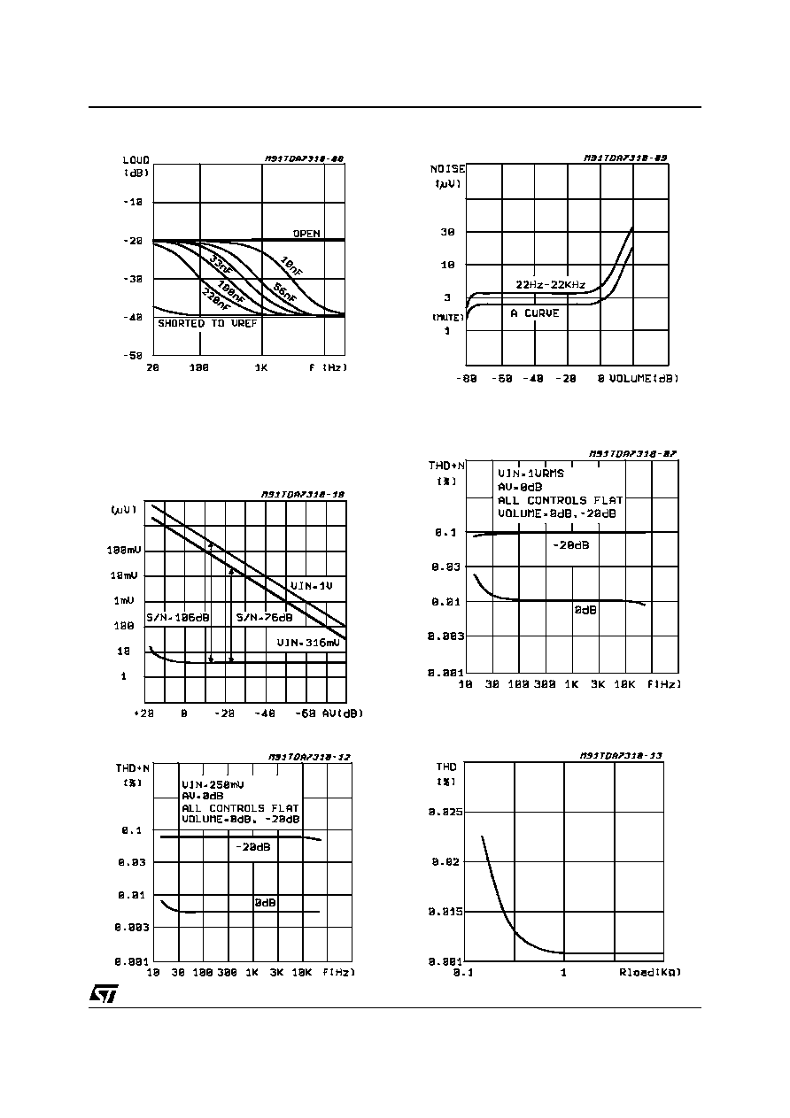
Figure 6: Distortion & Noise vs. Frequency
Figure 7: Distortion & Noise vs. Frequency
Figure 8: Distortion vs. Load Resistance
Figure 4: Noise vs. Volume/Gain Settings
Figure 5: Signal to Noise Ratio vs. Volume
Setting
Figure 3: Loudness versus External Capacitors
LOUDNESS
V
S
= 9V
Volume = -40dB
All other control flat
C
in
= 2.2
µ
F
C
loud
= 220nF, 100nF, 33nF, 10nF, Open, Shorter to Vref
TDA7315
5/12

Figure 11: Output Clipping Level vs. Supply
Voltage
Figure 13: Supply Current vs. Temperature
Figure 12: Quiescent Current vs. Supply Voltage
Figure 9: Channel Separation (L
R) vs.
Frequency
Figure 10: Supply Voltage Rejection vs.
Frequency
Figure 14: Bass Resistance vs. Temperature
TDA7315
6/12

SOFTWARE SPECIFICATION
Interface Protocol
The interface protocol comprises:
A start condition (S)
A chip address byte, containing the TDA7315
address (the 8th bit of the byte must be 0). The
TDA7315 must always acknowledge at the end
of each transmitted byte.
A sequence of data (N-bytes + acknowledge)
A stop condition (P)
TDA7315 ADDRESS
MSB
first byte
LSB
MSB
LSB
MSB
LSB
S
1
0
0
0
0
0
0
0
ACK
DATA
ACK
DATA
ACK
P
Data Transferred (N-bytes + Acknowledge)
ACK = Acknowledge
S = Start
P = Stop
MAX CLOCK SPEED 100kbits/s
SOFTWARE SPECIFICATION
Chip address = 80 Hex
1
MSB
0
0
0
0
0
0
0
LSB
DATA BYTES
MSB
LSB
FUNCTION
0
1
1
0
0
0
0
0
0
1
1
1
B2
0
1
0
1
1
B1
B1
B1
X
0
1
B0
B0
B0
X
C3
C3
A2
A2
A2
L
C2
C2
A1
A1
A1
X
C1
C1
A0
A0
A0
X
C0
C0
Volume control
Speaker ATT L
Speaker ATT R
Loudness
Bass control
Treble control
Ax = 1.25dB steps; Bx = 10dB steps; Cx = 2dB steps; X = don`t care.
Figure 15: Typical Tone Response (with the ext.
components indicated in the test
circuit)
TDA7315
7/12

SOFTWARE SPECIFICATION (continued)
DATA BYTES (detailed description)
Volume
MSB
LSB
FUNCTION
0
0
B2
B1
B0
A2
A1
A0
Volume 1.25dB steps
0
0
0
0
1
1
1
1
0
0
1
1
0
0
1
1
0
1
0
1
0
1
0
1
0
-1.25
-2.5
-3.75
-5
-6.25
-7.5
-8.75
0
0
B2
B1
B0
A2
A1
A0
Volume 10dB steps
0
0
0
0
1
1
1
1
0
0
1
1
0
0
1
1
0
1
0
1
0
1
0
1
0
-10
-20
-30
-40
-50
-60
-70
For example a volume of -45dB is given by:
0 0 1 0 0 1 0 0
Speaker Attenuators
MSB
LSB
FUNCTION
1
1
0
0
0
1
B1
B1
B0
B0
A2
A2
A1
A1
A0
A0
Speaker L
Speaker R
0
0
0
0
1
1
1
1
0
0
1
1
0
0
1
1
0
1
0
1
0
1
0
1
0
-1.25
-2.5
-3.75
-5
-6.25
-7.5
-8.75
0
0
1
1
0
1
0
1
0
-10
-20
-30
1
1
1
1
1
Mute
For example attenuation of 25dB on speaker R is given by:
1 0 1 1 0 1 0 0
TDA7315
8/12

Loudness
MSB
LSB
FUNCTION
0
1
0
X
X
L
X
X
0
1
LOUDNESS ON
LOUDNESS OFF
x = don`t care
For examples Loudness Off can be programmed by the following 8 bit string:
0 1 0 0 0 1 0 0
Bass and Treble
0
0
1
1
1
1
0
1
C3
C3
C2
C2
C1
C1
C0
C0
Bass
Treble
0
0
0
0
0
0
0
0
1
1
1
1
1
1
1
1
0
0
0
0
1
1
1
1
1
1
1
1
0
0
0
0
0
0
1
1
0
0
1
1
1
1
0
0
1
1
0
0
0
1
0
1
0
1
0
1
1
0
1
0
1
0
1
0
-14
-12
-10
-8
-6
-4
-2
0
0
2
4
6
8
10
12
14
C3 = Sign
For example Bass at -10dB is obtained by the following 8 bit string:
0 1 1 0 0 0 1 0
TDA7315
9/12

SO20 PACKAGE MECHANICAL DATA
DIM.
mm
inch
MIN.
TYP.
MAX.
MIN.
TYP.
MAX.
A
2.35
2.65
0.093
0.104
A1
0.1
0.3
0.004
0.012
B
0.33
0.51
0.013
0.020
C
0.23
0.32
0.009
0.013
D
12.6
13
0.496
0.512
E
7.4
7.6
0.291
0.299
e
1.27
0.050
H
10
10.65
0.394
0.419
h
0.25
0.75
0.010
0.030
L
0.4
1.27
0.016
0.050
K
0 (min.)8 (max.)
1
10
11
20
A
e
B
D
E
L
K
H
A1
C
SO20MEC
h x 45∞
TDA7315
10/12

DIP20 PACKAGE MECHANICAL DATA
DIM.
mm
inch
MIN.
TYP.
MAX.
MIN.
TYP.
MAX.
a1
0.254
0.010
B
1.39
1.65
0.055
0.065
b
0.45
0.018
b1
0.25
0.010
D
25.4
1.000
E
8.5
0.335
e
2.54
0.100
e3
22.86
0.900
F
7.1
0.280
I
3.93
0.155
L
3.3
0.130
Z
1.34
0.053
TDA7315
11/12

Information furnished is believed to be accurate and reliable. However, STMicroelectronics assumes no responsibility for the consequences
of use of such information nor for any infringement of patents or other rights of third parties which may result from its use. No license is
granted by implication or otherwise under any patent or patent rights of STMicroelectronics. Specification mentioned in this publication are
subject to change without notice. This publication supersedes and replaces all information previously supplied. STMicroelectronics products
are not authorized for use as critical components in life support devices or systems without express written approval of STMicroelectronics.
The ST logo is a registered trademark of STMicroelectronics
© 1998 STMicroelectronics ≠ Printed in Italy ≠ All Rights Reserved
STMicroelectronics GROUP OF COMPANIES
Australia - Brazil - Canada - China - France - Germany - Italy - Japan - Korea - Malaysia - Malta - Mexico - Morocco - The Netherlands -
Singapore - Spain - Sweden - Switzerland - Taiwan - Thailand - United Kingdom - U.S.A.
TDA7315
12/12