 | –≠–ª–µ–∫—Ç—Ä–æ–Ω–Ω—ã–π –∫–æ–º–ø–æ–Ω–µ–Ω—Ç: TDA7345 | –°–∫–∞—á–∞—Ç—å:  PDF PDF  ZIP ZIP |

TDA7345
DIGITALLY CONTROLLED AUDIO PROCESSOR
WITH SURROUND SOUND MATRIX
1 STEREO INPUT
VOLUME CONTROL IN 1.25dB STEP
TREBLE AND BASS CONTROL
THREE SURROUND MODES ARE AVAIL-
ABLE:
≠ MOVIE, MUSIC AND SIMULATED
FOUR SPEAKER ATTENUATORS:
≠ 4 INDEPENDENT SPEAKERS CONTROL
IN 1.25dB STEPS FOR BALANCE FACILITY
≠ INDEPENDENT MUTE FUNCTION
ALL FUNCTIONS PROGRAMMABLE VIA SE-
RIAL BUS
DESCRIPTION
The TDA7345 is a volume tone (bass and treble)
balance (Left/Right) processor for quality audio
applications in car radio and Hi-Fi systems.
It reproduces surround sound by using phase
shifters and a signal matrix. Control of all the
functions is accomplished by serial bus.
The AC signal setting is obtained by resistor net-
works and switches combined with operational
amplifiers.
Thanks to the used BIPOLAR/CMOS Technology,
Low Distortion, Low Noise and DC stepping are
obtained.
November 1999
Æ
HP2
L-in
BASS-LA
BASS-LB
TREBLE-L
REC_OUT_R
REC_OUT_L
Lout
Rout
1
3
2
4
5
6
7
8
9
AGND
SCL
SDA
TREBLE-R
DIG GND
BASS-RB
BASS-RA
R-in
REAR OUT
23
22
21
20
19
17
18
16
15
D94AU191A
10
11
12
13
14
28
27
26
25
24
CREF
PS2
PS1
LP1
HP1
REAR IN
LP
PS4
PS3
Vs
PIN CONNECTION
ORDERING NUMBER: TDA7345D
SO28
1/18

L-in
RLP1
L-R
0.47
µ
F
SUPPLY
V
S
AGND
CREF
VOL
100nF
BASS
5.6K
BASS-LA
BASS-LB
100nF
RB
TREBLE
5.6nF
TREBLE(L)
MUTE
D94AU192A
MUTE
I2
C
BUS
DECODER
+
LATCHES
SPKR
ATT
SPKR
ATT
VOL
BASS
TREBLE
100nF
100nF
5.6K
RB
5.6nF
TREBLE(R)
MUTE
SPKR
ATT
MUTE
SPKR
ATT
SCL
SDA
DIG
GND
ROUT
REC_
OUT_R
LOUT
REC_OUT_L
C5
22
µ
F
50K
+
-
+
-
+
RHP1
LP1
HP1
HP2
5.6nF
680nF
-
+
R6
R5
R-in
0.47
µ
F
50K
PS1
90Hz
100nF
PS1
RPS1
SIM
MOVIE/
MUSIC
MUSIC
OFF
PS2
4KHz
PS3
400Hz
PS4
400Hz
PHASE
SHIFTER
100nF
PS2
RPS2
22nF
PS3
RPS3
22nF
PS4
RPS4
MOVIE/SIM
MIXING
AMP
LPF
9KHz
EFFECT
CONTROL
MIXING
AMP
REAR
IN
1.2nF
LP
BASS-RA
BASS-RB
7
4
5
6
3
2
27
26
22
28
15
1
2
5
2
3
REAR
OUT
24
89
1
0
11
21
20
19
13
16
17
18
14
12
BLOCK DIAGRAM
TDA7345
2/18
680nF
C16
HP1
HP2
L-in
0.47
µ
F
C17
BASS-LA
C20 100nF
C21 100nF
BASS-LB
R2
5.6K
TREBLE-L
5.6nF
C22
LOUT
ROUT
AGND
SCL
SDA
DIG GND
LP1
PS1
PS2
CREF
VS
22nF C4
PS3
1.2nF
C6
LP
R-in
0.47
µ
F C7
BASS-RA
C10 100nF
C11 100nF
BASS-RB
R1
5.6K
TREBLE-R
5.6nF
C12
22nF C5
PS4
5.6nF C15 100nF C14
22
µ
F C3
100nF C2
100nF C13
10
µ
F C1
2.2
µ
F
REAR IN
REAR OUT
TDA7345
D94AU193A
5
6
7
8
9
10
13
14
15
17
16
18
25
24
23
22
21
20
19
26
27
1
28
2
3
4
REC OUT R
12
REC OUT L
11
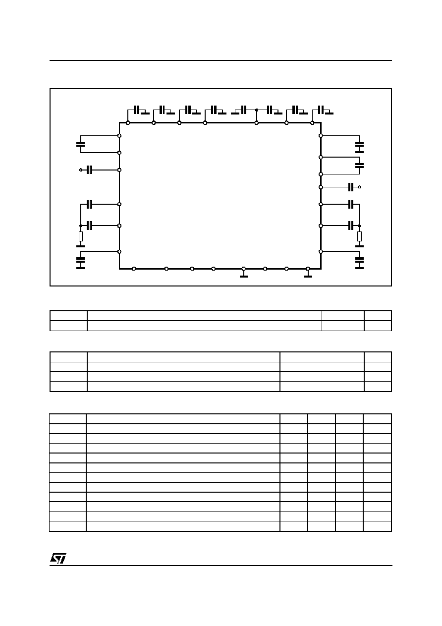
TEST CIRCUIT
THERMAL DATA
Symbol
Description
Value
Unit
R
th j-pins
Thermal Resistance Junction-pins
Ma x.
85
∞
C/W
QUICK REFERENCE DATA
Symbol
Parameter
Min.
Typ.
Max.
Unit
V
S
Supply Voltage
7
9
10.5
V
V
CL
Max. input signal handling
2
Vrms
THD
Total Harmonic Distortion V = 1Vrms f = 1KHz
0.02
0.1
%
S/N
Signal to Noise Ratio V
out
= 1Vrms (made = OFF)
106
dB
S
C
Channel Separation f = 1KHz
70
dB
Volume Control
1.25dB step
-78.75
0
dB
Treble Control
(2db step)
-14
+14
dB
Bass Control (2db step)
-14
+14
dB
Balance Control
1.25dB step REC-OUT L & R
-38.75
0
dB
Balance Control
1.25dB step (L
OUT,
R
OUT
)
-78.75
0
dB
Mute Attenuation
90
dB
ABSOLUTE MAXIMUM RATINGS
Symbol
Parameter
Value
Unit
V
S
Operating Supply Voltage
11
V
T
amb
Operating Ambient Temperature
-10 to 85
∞
C
T
stg
Storage Temperature Range
-55 to +150
∞
C
TDA7345
3/18
ELECTRICAL CHARACTERISTICS (refer to the test circuit T
amb
= 25
∞
C, V
S
= 9V, R
L
= 10K
,
R
G
= 600
, all controls flat (G = 0),Effect Ctrl = -6dB, MODE = OFF; f = 1KHz
unless otherwise specified)
Symbol
Parameter
Test Condition
Min.
Typ.
Max.
Unit
SUPPLY
V
S
Supply Voltage
7
9
10.5
V
I
S
Supply Current
20
25
35
mA
SVR
Ripple Rejection
L
CH
/ R
CH out
, Mode = OFF
60
80
dB
INPUT STAGE
R
II
Input Resistance
35
50
65
K
V
CL
Clipping Level
THD = 0.3%; Lin or Rin
2
2.5
Vrms
THD = 0.3%; Rin + Lin (2)
3.0
Vrms
C
RANGE
Control Range
19.68
dB
A
VMIN
Min. Attenuation
-1
0
1
dB
A
VMAX
Max. Attenuation
18.68
19.68
20.68
dB
A
STEP
Step Resolution
0.11
0.31
0.51
dB
V
DC
DC Steps
adjacent att. step
-3
0
3
mV
VOLUME CONTROL
C
RANGE
Control Range
70
75
dB
A
VMIN
Min. Attenuation
-1
0
1
dB
A
VMAX
Max. Attenuation
70
75
dB
A
STEP
Step Resolution
Av = 0 to -40dB
0.5
1.25
1.75
dB
E
A
Attenuation Set Error
Av = 0 to -20dB
Av = -20 to -60dB
-1.5
-3
0
1.5
2
dB
dB
E
T
Tracking Error
2
dB
V
DC
DC Steps
adjacent attenuation steps
-3
0
3
mV
BASS CONTROL (1)
Gb
Control Range
Max. Boost/cut
+11.5
+14.0
+16.0
dB
B
STEP
Step Resolution
1
2
3
dB
R
B
Internal Feedback Resistance
32
44
56
K
TREBLE CONTROL (1)
Gt
Control Range
Max. Boost/cut
+13
+14
+15
dB
T
STEP
Step Resolution
1
2
3
dB
EFFECT CONTROL
C
RANGE
Control Range
- 21
- 6
dB
S
STEP
Step Resolution
0.5
1
1.5
dB
TDA7345
4/18
ELECTRICAL CHARACTERISTICS (continued)
SURROUND SOUND MATRIX
Symbol
Parameter
Test Condition
Min.
Typ.
Max.
Unit
G
OFF
In-phase Gain (OFF)
Mode OFF , Input signal of
1kHz, 1.4 V
p-p
, R
in
R
out
L
in
L
out
-1.5
0
1.5
dB
D
GOFF
LR In-phase Gain Difference
(OFF)
Mode OFF , Input signal of
1kHz, 1.4 V
p-p
(R
in
R
out
), (L
in
L
out
)
-1.5
0
1.5
dB
G
MOV1
In-phase Gain (Movie 1)
Movie mode, Effect Ctrl = -6dB
Input signal of 1kHz, 1.4 V
p-p
R
in
R
out
, L
in
L
out
7
dB
G
MOV2
In-phase Gain (Movie 2)
Movie mode, Effect Ctrl = -6dB
Input signal of 1kHz, 1.4 V
p-p
R
in
R
out
, L
in
L
out
8
dB
D
GMOV
LR In-phase Gain Diffrence
(Movie)
Movie mode, Effect Ctrl = -6dB
Input signal of 1kHz, 1.4 V
p-p
(R
in
R
out
) ≠ (L
in
L
out
)
0
dB
G
MUS1
In-phase Gain (Music 1)
Music mode, Effect Ctrl = -6dB
Input signal of 1kHz, 1.4 V
p-p
(R
in
R
out
) ≠ (L
in
L
out
)
6
dB
G
MUS2
In-phase Gain (Music 2)
Music mode, Effect Ctrl = -6dB
Input signal of 1kHz, 1.4 V
p-p
R
in
R
out
, L
in
L
out
7.5
dB
D
GMUS
LR In-phase Gain Difference
(Music)
Music mode, Effect Ctrl = -6dB
Input signal of 1kHz, 1.4 V
p-p
(R
in
R
out
) ≠ (L
in
L
out
)
0
dB
L
MON1
Simulated L Output 1
Simulated Mode, Effect Ctrl = -6dB
Input signal of 250Hz,
1.4 V
p-p
, R
in
and L
in
L
ou t
4.5
dB
L
MON2
Simulated L Output 2
Simulated Mode, Effect Ctrl = -6dB
Input signal of 1kHz,
1.4 V
p-p
, R
in
and L
in
L
ou t
≠ 4.0
dB
L
MON3
Simulated L Output 3
Simulated Mode, EffectCtrl = -6dB
Input signal of 3.6kHz,
1.4 V
p-p
, R
in
and L
in
L
ou t
7.0
dB
R
MON1
Simulated R Output 1
Simulated Mode, Effect Ctrl = -6dB
Input signal of 250Hz,
1.4 V
p-p
, R
in
and L
in
R
out
≠ 4.5
dB
R
MON2
Simulated R Output 2
Simulated Mode, Effect Ctrl = -6dB
Input signal of 1kHz,
1.4 V
p-p
, R
in
and L
in
R
out
3.8
dB
R
MON3
Simulated R Output 3
Simulated Mode, Effect Ctrl = -6dB
Input signal of 3.6kHz,
1.4 V
p-p
, R
in
and L
in
R
out
≠ 20
dB
R
LP1
Low Pass Filter Resistance
7.5
10
12.5
K
R
PS1
Phase Shifter 1 Resistance
13.5
17.95
22.5
k
R
PS2
Phase Shifter 2 Resistance
0.30
0.40
0.50
K
R
PS3
Phase Shifter 3 Resistance
13.6
18.08
22.6
K
R
PS2
Phase Shifter 4 Resistance
13.6
18.08
22.6
K
R
HPI
High Pass Filter Resistance
45
60
75
K
R
LPF
LP Pin Impedance
7.5
10
12.5
K
TDA7345
5/18
ELECTRICAL CHARACTERISTICS (continued)
Symbol
Parameter
Test Condition
Min.
Typ.
Max.
Unit
SPEAKER ATTENUATORS (REC_OUT_L, REC_OUT_R)
C
range
Control Range
35
37.5
40
dB
S
STEP
Step Resolution
0.5
1.25
1.75
dB
E
A
Attenuation set error
-1.5
1.5
dB
A
MUTE
Output Mute Attenuation
80
90
dB
V
DC
DC Steps
adjacent att. steps
-3
0
3
mV
SPEAKER ATTENUATORS (LOUT, ROUT)
C
range
Control Range
70
75
dB
S
STEP
Step Resolution
Av = 0 to -40dB
0.5
1.25
1.75
dB
E
A
Attenuation set error
Av = 0 to 20dB
-1.5
0
1.5
dB
Av = -20 to -60dB
-3
0
2
dB
V
DC
DC Steps
adjacent att. steps
-3
0
3
mV
A
MUTE
Output Mute Attenuation
80
90
dB
AUDIO OUTPUTS (LOUT, ROUT, REC_OUT_L, REC_OUT_R)
V
OCL
Clipping Level
d = 0.3%
2
2.5
Vrms
R
OUT
Output resistance
100
200
300
V
OUT
DC Voltage Level
4.2
4.5
4.8
V
GENERAL
N
O(OFF)
Output Noise (OFF)
B
W
= 20Hz to 20KHz
Output LOUT, ROUT,
Output: REC-OUT-L,
REC-OUT-R
8
8
15
15
µ
Vrms
µ
Vrms
N
O(MOV)
Output Noise (Movie)
Mode =Movie ,
B
W
= 20Hz to 20KHz
R
out
and L
out
measurement
30
µ
Vrms
N
O(MUS)
Output Noise (Music)
Mode = Music ,
B
W
= 20Hz to 20KHz,
R
out
and L
out
measurement
30
µ
Vrms
N
O(MON)
Output Noise (Simulated)
Mode = Simulated,
B
W
= 20Hz to 20KHz
R
out
and L
out
measurement
30
µ
Vrms
d
Distorsion
Av = 0 ; V
in
= 1Vrms
0.02
0.1
%
S
C
Channel Separation
60
70
dB
BUS INPUTS
V
IL
Input Low Voltage
1
V
V
IH
Input High Voltage
3
V
I
IN
Input Current
-5
+5
µ
A
V
O
Output Voltage SDA
Acknowledge
I
O
= 1.6mA
0.4
0.8
V
Note:
(1) Bass and Treble response: The center frequency and the resonance quality can be choosen by
the external circuitry. A standard first order bass response can be realized by a standard feedback network.
(2) The peack voltage of the two input signals must be less then
V
S
2
:
(Lin + Rin)
peak
∑
A
Vin
<
V
S
2
TDA7345
6/18
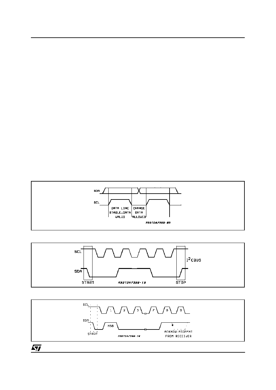
I
2
C BUS INTERFACE
Data transmission from microprocessor to the
TDA7345 and viceversa takes place through the
2 wires I
2
C BUS interface, consisting of the two
lines SDA and SCL (pull-up resistors to positive
supply voltage must be connected).
Data Validity
As shown in fig. 3, the data on the SDA line must
be stable during the high period of the clock. The
HIGH and LOW state of the data line can only
change when the clock signal on the SCL line is
LOW.
Start and Stop Conditions
As shown in fig.4 a start condition is a HIGH to
LOW transition of the SDA line while SCL is
HIGH. The stop condition is a LOW to HIGH tran-
sition of the SDA line while SCL is HIGH.
Byte Format
Every byte transferred on the SDA line must con-
tain 8 bits. Each byte must be followed by an ac-
knowledge bit. The MSB is transferred first.
Acknowledge
The master (
µ
P) puts a resistive HIGH level on the
SDA line during the acknowledge clock pulse (see
fig. 5). The peripheral (audioprocessor) that ac-
knowledges has to pull-down (LOW) the SDA line
during the acknowledge clock pulse, so that the
SDA line is stable LOW during this clock pulse.
The audioprocessor which has been addressed
has to generate an acknowledge after the recep-
tion of each byte, otherwise the SDA line remains
at the HIGH level during the ninth clock pulse
time. In this case the master transmitter can gen-
erate the STOP information in order to abort the
transfer.
Transmission without Acknowledge
Avoiding to detect the acknowledge of the audio-
processor, the
µ
P can use a simpler transmission:
simply it waits one clock without checking the
slave acknowledging, and sends the new data.
This approach of course is less protected from
misworking and decreases the noise immunity.
Figure 3: Data Validity on the I
2
CBUS
Figure 4: Timing Diagram of I
2
CBUS
Figure 5: Acknowledge on the I
2
CBUS
TDA7345
7/18
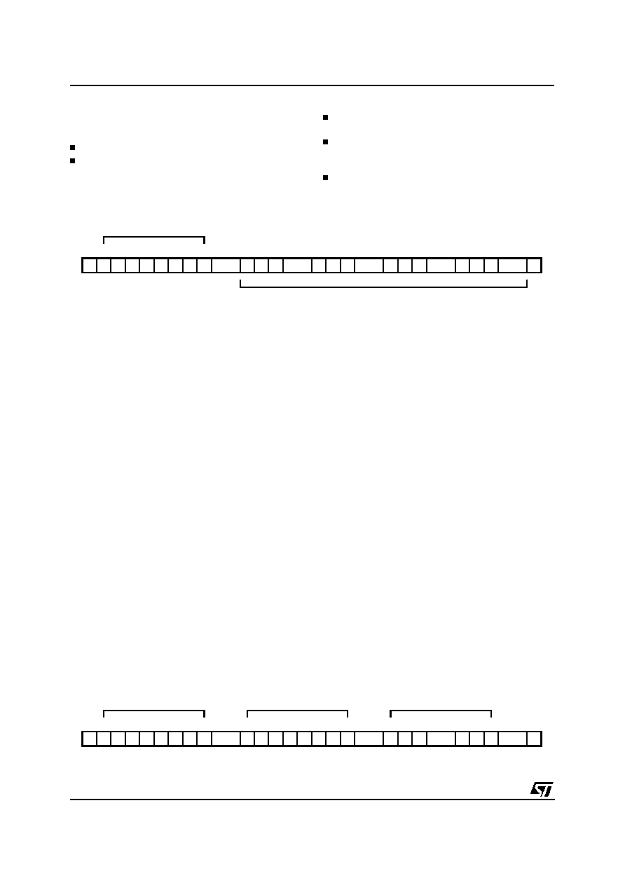
INTERFACE FEATURES
- Due to the fact that the MSB is used to select
if the byte transmitted is a subaddress (func-
tion) or a data (value), between a start and
stop condition, is possible to receive, how
many subaddresses and datas as wanted.
- The subaddress (function) is fixed until a new
subaddress is transmitted, so the TDA7345
can receive how many data as wanted for the
selected subaddress (without the need for a
new start condition)
- If TDA7345 receives a subaddress with the
LSB = 1 the incremental bus is selected, so it
enters in a loop condition that means that
every acknowledge will increase automat-
ically the subaddress (function) and it re-
ceives the data related to the new subad-
dress.
EXAMPLES
1) NO INCREMENTAL BUS
TDA7345 receives a start condition, the correct
chip address, a subaddress with the LSB = 0 (no
incremental bus), N-datas (all these datas con-
cern the subaddress selected), a new subad-
dress, N-data, a stop condition.
So it can receive in a single transmission how
many subaddress are necessary, and for each
subaddress how many data are necessary.
2) INCREMENTAL BUS
TDA7345 receives a start condition, the correct
chip address a subaddress with the LSB = 1 (in-
cremental bus): now it is in a loop condition with
an autoincrease of the subaddress.
The first data that it receives doesn't concern the
subaddress sended but the next one, the second
one concerns the subaddress sended plus two in
the loop etc, and at the end it receives the stop
condition.
In the pictures there are some examples:
S = start
ACK = acknowledge
B = 1 incremental bus, B = 0 no incremental bus
P = stop
SOFTWARE SPECIFICATION
Interface Protocol
The interface protocol comprises:
A start condition (s)
A chip address byte, containing the TDA7345
address (the 8th bit of the byte must be 0).
The TDA7345 must always acknowledge at
the end of each transmitted byte.
A subaddress (function) bytes (identified by the
MSB = 0)
A sequence of dates and subaddresses (N
bytes + achnowledge. The dates are identified
by MSB = 1, subaddresses by MSB = 0)
A stop condition (P)
S
1
0
0
0
0
0
1
0
ACK
A2
ACK
DATA
ACK
P
MSB
LSB
MSB
LSB
MSB
LSB
CHIP ADDRESS
D94AU195
0 A0 A1
A3 X
X
0
1
SUBADDRESS
DATA 1 ... DATA n
1) one subaddress, with n data concerning that subaddress (no incremental bus)
ACK = Achnowledge
S = Start
P = Stop
S
1
0
0
0
0
0
1
0
ACK
DATA
ACK
DATA
ACK
S
MSB
LSB
MSB
LSB
MSB
LSB
Data Transferred (N-bytes + Acknowledge)
TDA7345 ADDRESS
D94AU194
TDA7345
8/18
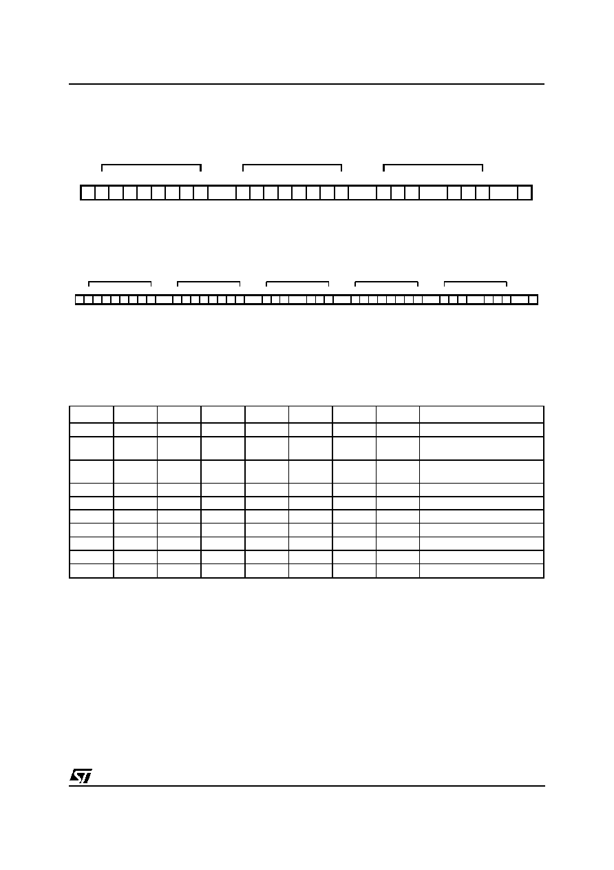
MSB
LSB
SUBADDRESS
A0
A1
A2
A3
B
0
0
0
0
X
X
X
B
VOLUME ATTENUATION &
LOUDNESS
0
1
0
0
X
X
X
B
SURROUND & OUT &
EFFECT CONTROL
0
0
1
0
X
X
X
B
BASS
0
1
1
0
X
X
X
B
TREBLE
0
0
0
1
X
X
X
B
REC-OUT-R
0
1
0
1
X
X
X
B
REC-OUT-L
0
0
1
1
X
X
X
B
R
OUT
0
1
1
1
0
X
X
B
L
OUT
0
1
1
1
1
X
X
B
INPUT STAGE CONTROL
B = 1 yes incremental bus;
B = 0 no incremental bus;
X = indifferent 0,1
The first byte select the function, it is identified by the MSB = 0
DATA BYTES
FUNCTION SELECTION
FIRST BYTE (subaddress)
S
1
0
0
0
0
0
1
0
ACK
A2
ACK
DATA
ACK
P
MSB
LSB
MSB
LSB
MSB
LSB
CHIP ADDRESS
D94AU196
0 A0 A1
A3 X
X
1
1
SUBADDRESS
DATA 1 ... DATA n
2) one subaddress, (with incremental bus) , with n data (data1 that concerns subaddress +1, data 2
that concerns subaddress + 2 etc.)
S
1
0
0
0
0
0
1
0
ACK
A2
ACK
DATA
MSB
LSB
MSB
LSB
MSB
LSB
CHIP ADDRESS
D94AU197
0 A0 A1
A3 X
X
0
1
SUBADDRESS
DATA 1 ... DATA n
ACK
A2
ACK
DATA
ACK
1
MSB
LSB
MSB
LSB
0 A0 A1
A3 X
X
0
1
SUBADDRESS
DATA 1 ... DATA n
3) more subaddress with more data
TDA7345
9/18
VOLUME ATTENUATION
MSB
LSB
1.25 dB STEPS
1
0
0
0
0
1
0
0
1
-1.25
1
0
1
0
-2.50
1
0
1
1
-3.75
1
1
0
0
-5.00
1
1
0
1
-6.25
1
1
1
0
-7.50
1
1
1
1
-8.75
10 dB STEPS
1
0
0
0
0
1
0
0
1
-10
1
0
1
0
-20
1
0
1
1
-30
1
1
0
0
-40
1
1
0
1
-50
1
1
1
0
-60
1
1
1
1
-70
ATT SPEAKER L AND R
MSB
LSB
1.25 dB STEPS
1
0
0
0
0
1
0
0
1
-1.25
1
0
1
0
-2.50
1
0
1
1
-3.75
1
1
0
0
-5.00
1
1
0
1
-6.25
1
1
1
0
-7.50
1
1
1
1
-8.75
10 dB STEPS
1
0
0
0
0
1
0
0
1
-10
1
0
1
0
-20
1
0
1
1
-30
1
1
0
0
-40
1
1
0
1
-50
1
1
1
0
-60
1
1
1
1
-70
MUTE
1
0
OFF
1
1
ON
VALUE SELECTION
The second byte select the value, it is identified by the MSB = 1
TDA7345
10/18
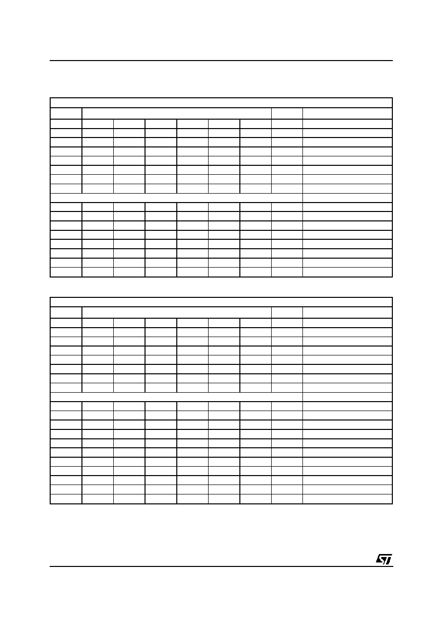
ATT REC-OUT L AND R
MSB
LSB
1.25 dB STEPS
1
X
X
0
0
0
0
1
X
X
0
0
1
-1.25
1
X
X
0
1
0
-2.50
1
X
X
0
1
1
-3.75
1
X
X
1
0
0
-5.00
1
X
X
1
0
1
-6.25
1
X
X
1
1
0
-7.50
1
X
X
1
1
1
-8.75
10 dB STEPS
1
X
X
0
0
0
1
X
X
0
1
-10
1
X
X
1
0
-20
1
X
X
1
1
-30
1
X
X
1
1
1
1
1
MUTE
TREBLE/ BASS
MSB
LSB
2 dB STEPS
1
X
X
X
0
1
1
1
14
1
X
X
X
0
1
1
0
12
1
X
X
X
0
1
0
1
10
1
X
X
X
0
1
0
0
8
1
X
X
X
0
0
1
1
6
1
X
X
X
0
0
1
0
4
1
X
X
X
0
0
0
1
2
1
X
X
X
0
0
0
0
0
1
X
X
X
1
0
0
0
0
1
X
X
X
1
0
0
1
-2
1
X
X
X
1
0
1
0
-4
1
X
X
X
1
0
1
1
-6
1
X
X
X
1
1
0
0
-8
1
X
X
X
1
1
0
1
-10
1
X
X
X
1
1
1
0
-12
1
X
X
X
1
1
1
1
-14
TDA7345
11/18

SURROUND & OUT & EFFECT CONTROL
MSB
LSB
SELECTION
SELECTION
SURROUND
1
0
0
SIMULATED
1
0
1
MUSIC
1
1
0
MOVIE
1
1
1
OFF
SELECTION
EFFECT CONTROL
1
0
0
0
0
-6
1
0
0
0
1
-7
1
0
0
1
0
-8
1
0
0
1
1
-9
1
0
1
0
0
-10
1
0
1
0
1
-11
1
0
1
1
0
-12
1
0
1
1
1
-13
1
1
0
0
0
-14
1
1
0
0
1
-15
1
1
0
1
0
-16
1
1
0
1
1
-17
1
1
1
0
0
-18
1
1
1
0
1
-19
1
1
1
1
0
-20
1
1
1
1
1
-21
For example to select the music mode, out fix, effect control =-9dB:
1 0 0 1 1 1 0 1
TDA7345
12/18
INPUT CONTROL RANGE (0 TO -19.68dB)
MSB
LSB
0.3125 dB STEPS
1
X
0
0
0
0
1
Xx
0
0
1
-0.3125
1
X
0
1
0
-0.625
1
X
0
1
1
-0.9375
1
X
1
0
0
-1.25
1
X
1
0
1
-1.5625
1
X
1
1
0
-1.875
1
X
1
1
1
-2.1875
2.5 dB STEPS
1
X
0
0
0
0
1
X
0
0
1
-2.5
1
X
0
1
0
-5.0
1
X
0
1
1
-7.5
1
X
1
0
0
-10
1
X
1
0
1
-12.5
1
X
1
1
0
-15
1
X
1
1
1
-17.5
POWER ON RESET
VOLUME ATTENUATION
MAX ATTENUATION,
TREBLE
-14dB
BASS
-14dB
SURROUND + EFFECT CONTROL
OFF + MAX ATTENUATION
ATT SPEAKER R
MUTE
ATT SPEAKER L
MUTE
ATT REC-OUT L
MUTE
ATT REC-OUT R
MUTE
TDA7345
13/18
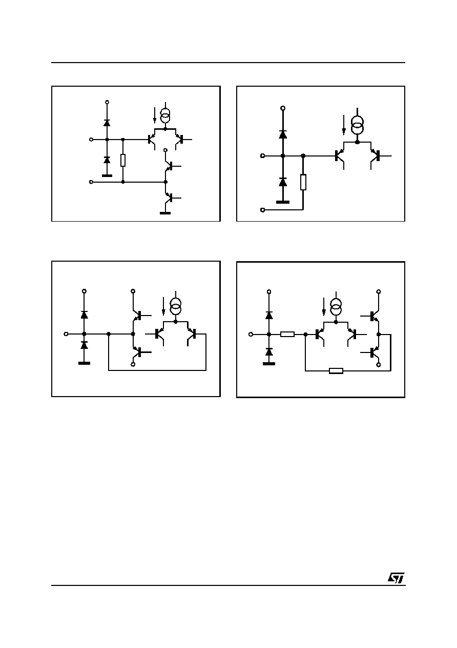
48K
GND
V
S
BASS-RB
D94AU201
20
µ
A
BASS-LB
PIN: BASS - LA, BASS - RA
50K
GND
V
S
V
REF
D94AU200
20
µ
A
PIN: L
in
, R
in
25K
V
S
D94AU203
20
µ
A
PIN: TREBLE - L, TREBLE - R
48K
GND
V
S
BASS-RA
D94AU202
20
µ
A
BASS-LA
PIN: BASS - LB, BASS - RB
10K
60K
GND
V
S
LP1
HP2
D94AU198
PIN: HP1
5.5K
60K
GND
V
S
HP1
D94AU199
20
µ
A
5.5K
PIN: HP2
TDA7345
14/18
18.08K
V
S
D94AU207
20
µ
A
PS3A
PS4A
PIN: PS3, PS2
10K
GND
V
S
D94AU206
20
µ
A
PIN: LP
398
V
S
D94AU209
20
µ
A
PS2A
PIN: PS2
50K
V
S
D94AU208
20
µ
A
50K
PIN: C
REF
100
V
S
D94AU204
20
µ
A
PIN: L
OUT
, R
OUT
, REC-OUT-1 REC-OUT-R
D94AU205
20
µ
A
PIN: SCL, SDA
TDA7345
15/18
17.95K
V
S
D94AU210
20
µ
A
PS1A
PIN: PS1
10K
V
S
D94AU211
20
µ
A
HP1
PIN: LP1
20K
V
S
D94AU215
20
µ
A
20K
PIN: REAR IN
V
S
D94AU214
20
µ
A
PIN: REAR OUT
TDA7345
16/18

SO28
DIM.
mm
inch
MIN.
TYP.
MAX.
MIN.
TYP.
MAX.
A
2.65
0.104
a1
0.1
0.3
0.004
0.012
b
0.35
0.49
0.014
0.019
b1
0.23
0.32
0.009
0.013
C
0.5
0.020
c1
45
∞
(typ.)
D
17.7
18.1
0.697
0.713
E
10
10.65
0.394
0.419
e
1.27
0.050
e3
16.51
0.65
F
7.4
7.6
0.291
0.299
L
0.4
1.27
0.016
0.050
S
8
∞
(max.)
OUTLINE AND
MECHANICAL DATA
TDA7345
17/18

Information furnished is believed to be accurate and reliable. However, STMicroelectronics assumes no responsibility for the consequences
of use of such information nor for any infringement of patents or other rights of third parti es which may result from its use. No license is
granted by implication or otherwise under any patent or patent rights of STMicroelectronics. Specification mentioned in this publication are
subject to change without notice. This publication supersedes and replaces all information previously supplied. STMicroelectronics products
are not authorized for use as critical components in life support devices or systems without express written approval of STMicroelectronics.
The ST logo is a registered trademark of STMicroelectronics
©
1999 STMicroelectronics ≠ Printed in Italy ≠ All Rights Reserved
STMicroelectronics GROUP OF COMPANIES
Australia - Brazil - China - Finland - France - Germany - Hong Kong - India - Italy - Japan - Malaysia - Malta - Morocco -
Singapore - Spain - Sweden - Switzerland - United Kingdom - U.S.A.
http://www.st.com
TDA7345
18/18