 | –≠–ª–µ–∫—Ç—Ä–æ–Ω–Ω—ã–π –∫–æ–º–ø–æ–Ω–µ–Ω—Ç: TDA7374 | –°–∫–∞—á–∞—Ç—å:  PDF PDF  ZIP ZIP |

TDA7374B
DUAL BRIDGE AUDIO AMPLIFIER FOR CAR RADIO
MINIMUM EXTERNAL COMPONENT COUNT
NO BOOTSTRAP CAPACITORS
NO BOUCHEROT CELLS
CLIP DETECTOR OUTPUT
HIGH OUTPUT POWER
FIXED GAIN
VERY LOW STAND-BY CURRENT (1
µ
A typ)
NO SWITCH ON/OFF NOISE
PROTECTIONS:
OUTPUT AC/DC SHORT CIRCUIT TO GND
AND TO V
S
VERY INDUCTIVE LOADS
OVERRATING CHIP TEMPERATURE
LOAD DUMP VOLTAGE
FORTUITOUS OPEN GND
REVERSE BATTERY
ESD
DESCRIPTION
The TDA7374B is a new technology class AB
Audio Dual Bridge Power Amplifier in Multiwatt
package designed for car radio applications.
Thanks to the fully complementary PNP/NPN out-
put configuration the high power performances of
the TDA7374B are obtained without bootstrap ca-
pacitors.
April 1995
TEST AND APPLICATION CIRCUIT
MULTIWATT 15
ORDERING NUMBERS: TDA7374BV
1/13

PIN CONNECTION (Top view)
ABSOLUTE MAXIMUM RATINGS
Symbol
Parameter
Value
Unit
V
S
DC Supply Voltage
28
V
V
OP
Operating Supply Voltage
18
V
V
PEAK
Peak Supply Voltage (t = 50ms)
50
V
I
O
Output Peak Current (not rep. t = 100
µ
s)
4.5
A
I
O
Output Peak Current (rep. f > 10Hz)
3.5
A
P
tot
Power Dissipation (T
case
= 85
∞
C)
36
W
T
stg
, T
j
Storage and Junction Temperature
-40 to 150
∞
C
THERMAL DATA
Symbol
Description
Value
Unit
R
th j-case
Thermal Resistance Junction-case
Max
1.8
∞
C/W
TDA7374B
2/13
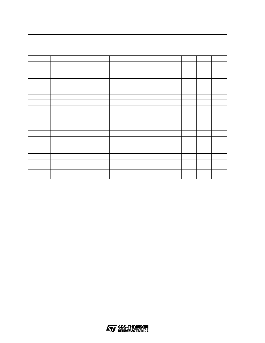
ELECTRICAL CHARACTERISTICS (Refer to the test circuit; V
S
= 14.4V; R
L
= 4
, T
amb
= 25
∞
C,
f = 1kHz, unless otherwise specified)
Symbol
Parameter
Test Condition
Min.
Typ.
Max.
Unit
V
S
Supply Range
8
18
V
I
d
Total Quiescent Drain Current
R
L
=
150
mA
P
O
Output Power
R
L
= 4
; THD = 10%
17
21
W
d
Distortion
R
L
= 4
P
O
= 0.1 to 10W
0.5
%
CT
Cross-Talk
f = 1kHz
f = 10kHz
65
55
dB
dB
R
IN
Input Impedance
10
K
G
V
Voltage Gain
26
dB
G
V
Voltage Gain Match.
1
dB
E
IN
Input Noise Voltage
R
g
= 0 to 10k
Weight A
22Hz to 22KHz
3.5
10
µ
V
µ
V
SVR
Supply Voltage Rejection
R
g
= 0; f = 100Hz
f = 10kHz
48
55
dB
ASB
Stand-by Attenuation
60
dB
I
SB
ST-BY Current
1
µ
A
V
SB ON
ST-BY On Threshold Voltage
1.5
V
V
SB OFF
ST-BY Off Threshold Voltage
3.5
V
V
OS
Output Offset Voltage
200
mV
I
CD OFF
Clipping Detector "OFF "
Output Average Current
THD = 1% (*)
100
µ
A
I
CD ON
Clipping Detector "ON"
Output Average Current
THD = 10% (*)
190
µ
A
(*) Pin 10 Pulled-up to 5V with 10k
; R
L
= 4
TDA7374B
3/13

TEST AND APPLICATION CIRCUIT
P.C. BOARD AND COMPONENT LAYOUT (1:1 scale)
B
TDA7374B
4/13

Figure 1: Quiescent Drain Current vs. Supply
Voltage
Figure 2: Quiescent Output Voltage vs. Supply
Voltage
Figure 3: Output Power vs. Supply Voltage
Figure 5: Output Power vs. Frequency
Figure 4: Distortion vs. Output Power
Figure 6: Supply Voltage Rejection vs.
Frequency for a Different values of C6
Capacitor
R
g
TDA7374B
5/13