 | –≠–ª–µ–∫—Ç—Ä–æ–Ω–Ω—ã–π –∫–æ–º–ø–æ–Ω–µ–Ω—Ç: TDA7375A | –°–∫–∞—á–∞—Ç—å:  PDF PDF  ZIP ZIP |

TDA7375A
2 x 37W DUAL/QUAD POWER AMPLIFIER FOR CAR RADIO
HIGH OUTPUT POWER CAPABILITY
2
x
43W/4
MAX
2
x
37W/4
EIAJ
2
x
26W/4
@14.4V, 1KHz, 10%
4
x
7W/4
@14.4V, 1KHz, 10%
4
x
12W/2
@14.4V, 1KHz, 10%
MINIMUM
EXTERNAL
COMPONENTS
COUNT:
≠ NO BOOTSTRAP CAPACITORS
≠ NO BOUCHEROT CELLS
≠ INTERNALLY FIXED GAIN (26dB BTL)
ST-BY FUNCTION (CMOS COMPATIBLE)
NO AUDIBLE POP DURING ST-BY OPERA-
TIONS
DIAGNOSTIC FACILITIES
≠ CLIP DETECTOR
≠ OUT TO GND SHORT
≠ OUT TO V
S
SHORT
≠ SOFT SHORT AT TURN-ON
≠ THERMAL SHUTDOWN PROXIMITY
Protections:
OUPUT AC/DC SHORT CIRCUIT
≠ TO GND
≠ TO V
S
≠ ACROSS THE LOAD
SOFT SHORT AT TURN-ON
OVERRATING CHIP TEMPERATURE WITH
SOFT THERMAL LIMITER
LOAD DUMP VOLTAGE SURGE
VERY INDUCTIVE LOADS
FORTUITOUS OPEN GND
REVERSED BATTERY
ESD
October 1998
Æ
Multiwatt15 V
BLOCK DIAGRAM
ORDERING NUMBERS: TDA7375AV
TDA7375AH
1/14
DESCRIPTION
The TDA7375A is a new technology class AB car
radio amplifier able to work either in DUAL
BRIDGE or QUAD SINGLE ENDED configuration.
The exclusive fully complementary structure of the
output stage and the internally fixed gain guaran-
tee the highest power performances with ex-
tremely reduced component count. The on board
clip detector simplifies gain compression opera-
tion. The fault diagnostic makes it possible to de-
tect mistakes during car radio set assembly and
wiring in the car.
GENERAL STRUCTURE
ABSOLUTE MAXIMUM RATINGS
Symbol
Parameter
Value
Unit
V
op
Operating Supply Voltage
18
V
V
S
DC Supply Voltage
28
V
V
peak
Peak Supply Voltage (for t = 50ms)
40
V
I
O
Output Peak Current (not repitive t = 100
µ
s)
4.5
A
I
O
Output Peak Current (repetitive f > 10Hz)
3.5
A
P
tot
Power Dissipation T
case
= 85
∞
C
36
W
T
stg
, T
j
Storage and Junction Temperature
-40 to 150
∞
C
THERMAL DATA
Symbol
Description
Value
Unit
R
th j-case
Thermal Resistance Junction-case
Max
1.8
∞
C/W
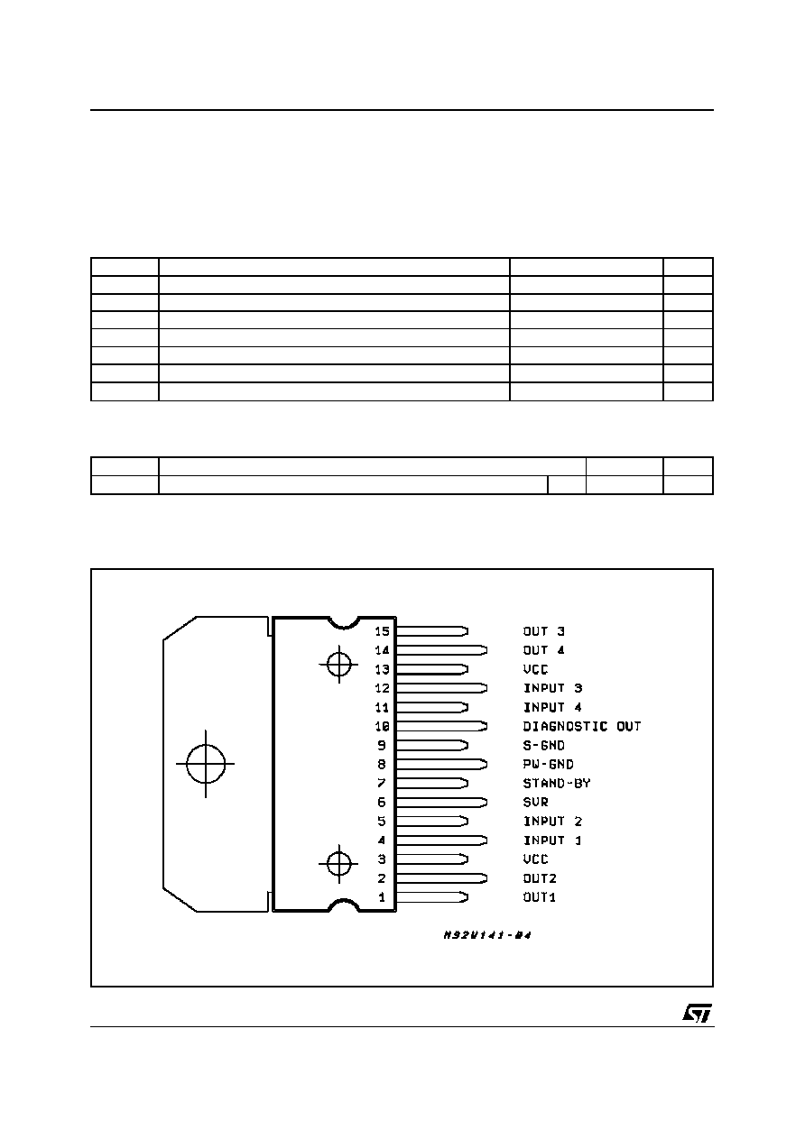
PIN CONNECTION (Top view)
TDA7375A
2/14
ELECTRICAL CHARACTERISTICS (Refer to the test circuit, V
S
= 14.4V; R
L
= 4
; f = 1KHz;
T
amb
= 25
∞
C, unless otherwise specified
Symbol
Parameter
Test Condition
Min.
Typ.
Max.
Unit
V
S
Supply Voltage Range
8
18
V
I
d
Total Quiescent Drain Current
R
L
=
150
mA
V
OS
Output Offset Voltage
150
mV
P
O
Output Power
THD = 10%; R
L
= 4
Bridge
Single Ended
Single Ended, R
L
= 2
23
6.5
26
7
12
W
W
W
P
O max
Max. Output Power (***)
VS = 14.4V, Bridge
37
43
W
P
O EIAJ
EIAJ Output Power (***)
V
S
= 13.7V, Bridge
33
37
W
THD
Distortion
R
L
= 4
Single Ended, P
O
= 0.1 to 4W
Bridge, P
O
= 0.1 to 10W
0.02
0.03
0.3
%
%
CT
Cross Talk
f = 1KHz Single Ended
f = 10KHz Single Ended
70
60
dB
dB
f = 1KHz Bridge
f = 10KHz Bridge
55
60
dB
dB
R
IN
Input Impedance
Single Ended
Bridge
20
10
30
15
K
K
G
V
Voltage Gain
Single Ended
Bridge
19
25
20
26
21
27
dB
dB
G
V
Voltage Gain Match
0.5
dB
E
IN
Input Noise Voltage
R
g
= 0; "A" weighted, S.E.
Non Inverting Channels
Inverting Channels
2
5
µ
V
µ
V
Bridge
Rg = 0; 22Hz to 22KHz
3.5
µ
V
SVR
Supply Voltage Rejection
R
g
= 0; f = 300Hz
50
dB
A
SB
Stand-by Attenuation
P
O
= 1W
80
90
dB
I
SB
ST-BY Current Consumption
V
ST-BY
= 0 to 1.5V
100
µ
A
V
SB
ST-BY In Threshold Voltage
1.5
V
V
SB
ST-BY Out Threshold Voltage
3.5
V
I
pin7
ST-BY Pin Current
Play Mode V
pin7
= 5V
50
µ
A
Max Driving Current Under
Fault (*)
5
mA
I
cd off
Clipping Detector
Output Average Current
d = 1% (**)
90
µ
A
I
cd on
Clipping Detector
Output Average Current
d = 5% (**)
160
µ
A
V
sat pin10
Voltage Saturation on pin 10
Sink Current at Pin 10 = 1mA
0.7
V
(*) See built-in S/C protection description
(**) Pin 10 Pulled-up to 5V with 10K
; R
L
= 4
(***) Saturated square wave output.
TDA7375A
3/14

C1 0.22
µ
F
1
DIAGNOSTICS
4
7
C10 2200
µ
F
D94AU063A
C7
10
µ
F
10K R1
ST-BY
IN FL
C2 0.22
µ
F
IN FR
5
C4 0.22
µ
F
12
IN RL
C3 0.22
µ
F
IN RR
11
C8 47
µ
F
6
13
C5
1000
µ
F
C6
100nF
3
VS
C9 2200
µ
F
2
15
C11 2200
µ
F
C12 2200
µ
F
14
OUT FL
OUT FR
OUT RL
OUT RR
8
9
10
STANDARD TEST AND APPLICATION CIRCUIT
Figure 1: Quad Stereo
C1 0.47
µ
F
1
DIAGNOSTICS
4
7
D94AU064A
C5
10
µ
F
10K R1
ST-BY
IN L
C2 0.47
µ
F
5
12
IN R
11
C8 47
µ
F
6
13
C3
1000
µ
F
C4
100nF
3
VS
2
15
14
OUT L
8
9
10
OUT R
Figure 2: Double Bridge
0.22
µ
F
1
DIAGNOSTICS
4
7
D94AU065A
10
µ
F
10K
ST-BY
IN L
0.47
µ
F
5
IN BRIDGE
12
47
µ
F
6
13
1000
µ
F
100nF
3
VS
2
15
14
OUT L
8
9
10
OUT
BRIDGE
11
0.22
µ
F
IN L
OUT R
2200
µ
F
2200
µ
F
Figure 3: Stereo/Bridge
Note:
The output decoupling capacitors
(C9,C10,C11,C12) could be reducedto
1000
µ
F if t he 2
operation is not
required.
TDA7375A
4/14
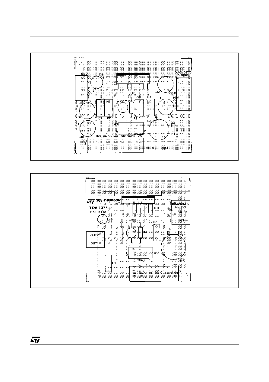
Figure 4: P.C. Board and Component Layout of the fig.1 (1:1 scale).
Figure 5: P.C. Board and Component Layout of the fig.2 (1:1 scale).
TDA7375A
5/14