 | –≠–ª–µ–∫—Ç—Ä–æ–Ω–Ω—ã–π –∫–æ–º–ø–æ–Ω–µ–Ω—Ç: TDA7439DS | –°–∫–∞—á–∞—Ç—å:  PDF PDF  ZIP ZIP |

TDA7439DS
THREE BANDS
DIGITALLY CONTROLLED AUDIO PROCESSOR
INPUT MULTIPLEXER
- 4 STEREO INPUTS
- SELECTABLE INPUT GAIN FOR OPTIMAL
ADAPTATION TO DIFFERENT SOURCES
ONE STEREO OUTPUT
TREBLE, MIDDLE AND BASS CONTROL IN
2.0dB STEPS
VOLUME CONTROL IN 1.0dB STEPS
TWO SPEAKER ATTENUATORS:
- TWO INDEPENDENT SPEAKER CONTROL
IN 1.0dB STEPS FOR BALANCE FACILITY
- INDEPENDENT MUTE FUNCTION
ALL FUNCTION ARE PROGRAMMABLE VIA
SERIAL BUS
DESCRIPTION
The TDA7439DS is a volume tone (bass, middle
and treble) balance (Left/Right) processor for
quality audio applications in car-radio and Hi-Fi
systems.
Selectable input gain is provided. Control of all
the functions is accomplished by serial bus.
The AC signal setting is obtained by resistor net-
works and switches combined with operational
amplifiers.
Thanks to the used BIPOLAR/CMOS Technology,
Low Distortion, Low Noise and DC stepping are
obtained
April 1999
0/30dB
2dB STEP
MUXOUTL
VOLUME
VOLUME
TREBLE
TREBLE
TREBLE(L)
MIDDLE
MIDDLE
MUXOUTR
TREBLE(R)
BOUT(L)
SPKR ATT
LEFT
LOUT
SCL
SDA
DIG_GND
ROUT
D97AU621
I
2
CBUS DECODER + LATCHES
100K
100K
100K
100K
G
L-IN1
L-IN2
L-IN3
L-IN4
100K
100K
100K
100K
R-IN1
R-IN2
R-IN3
R-IN4
G
INPUT MULTIPLEXER
+ GAIN
MOUT(L)
BASS
BIN(L)
BASS
SPKR ATT
RIGHT
MIN(R) MOUT(R)
BOUT(R)
BIN(R)
SUPPLY
CREF
AGND
V
S
MIN(L)
27
4
5
6
7
3
2
1
28
21
22
20
26
24
25
9
19
10
11
12
13
23
8
18
17
16
14
15
R
M
R
B
R
M
R
B
V
REF
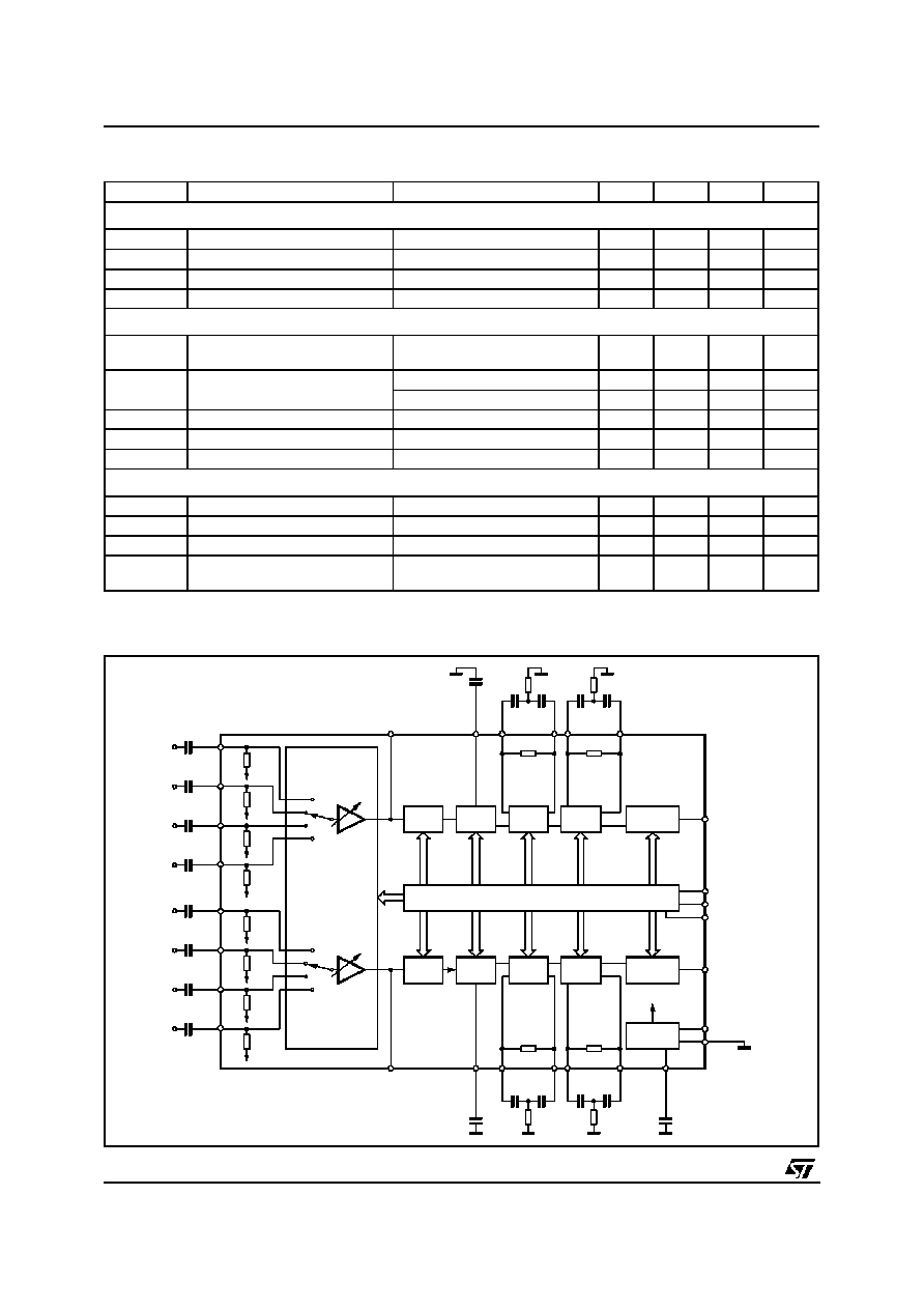
BLOCK DIAGRAM
ORDERING NUMBERS: TDA7439DS
SO28
Æ
1/16

L_IN3
L_IN4
MUXOUTL
MUXOUTR
MIN(R)
BIN(R)
MOUT(R)
BOUT(R)
BIN(L)
1
3
2
4
5
6
7
8
9
BOUT(L)
MOUT(L)
MIN(L)
TREBLE(R)
TREBLE(L)
SCL
SDA
DIG-GND
CREF
23
22
21
20
19
17
18
16
15
D97AU622
10
11
12
13
14
28
27
26
25
24
R_IN3
R_IN2
R_IN1
L_IN1
L_IN2
V
S
AGND
ROUT
LOUT
R_IN4
PIN CONNECTION
ABSOLUTE MAXIMUM RATINGS
Symbol
Parameter
Value
Unit
V
S
Operating Supply Voltage
10.5
V
T
amb
Operating Ambient Temperature
-10 to 85
∞
C
T
stg
Storage Temperature Range
-55 to 150
∞
C
THERMAL DATA
Symbol
Parameter
Value
Unit
R
th j-pin
Thermal Resistance Junction-pins
85
∞
C/W
QUICK REFERENCE DATA
Symbol
Parameter
Min.
Typ.
Max.
Unit
V
S
Supply Voltage
7
9
10.2
V
V
CL
Max. input signal handling
2
Vrms
THD
Total Harmonic Distortion V = 1Vrms f = 1KHz
0.01
0.1
%
S/N
Signal to Noise Ratio V
out
= 1Vrms (mode = OFF)
106
dB
S
C
Channel Separation f = 1KHz
90
dB
Input Gain in (2dB step)
0
30
dB
Volume Control
(1dB step)
-47
0
dB
Treble Control
(2dB step)
-14
+14
dB
Middle Control (2dB step)
-14
+14
dB
Bass Control (2dB step)
-14
+14
dB
Balance Control
1dB step
-79
0
dB
Mute Attenuation
100
dB
Æ
TDA7439DS
2/16

ELECTRICAL CHARACTERISTICS (refer to the test circuit T
amb
= 25
∞
C, V
S
= 9V, R
L
= 10K
,
R
G
= 600
, all controls flat (G = 0dB), unless otherwise specified)
Symbol
Parameter
Test Condition
Min.
Typ.
Max.
Unit
SUPPLY
V
S
Supply Voltage
7
9
10.2
V
I
S
Supply Current
4
7
10
mA
SVR
Ripple Rejection
60
90
dB
INPUT STAGE
R
IN
Input Resistance
70
100
130
K
V
CL
Clipping Level
THD = 0.3%
2
2.5
Vrms
S
IN
Input Separation
The selected input is grounded
through a 2.2
µ
capacitor
80
100
dB
G
inmin
Minimum Input Gain
-1
0
1
dB
G
inman
Maximum Input Gain
29
30
31
dB
G
step
Step Resolution
1.5
2
2.5
dB
VOLUME CONTROL
R
i
Input Resistance
20
33
50
K
C
RANGE
Control Range
45
47
49
dB
A
VMAX
Max. Attenuation
45
47
49
dB
A
STEP
Step Resolution
0.5
1
1.5
dB
E
A
Attenuation Set Error
A
V
= 0 to -24dB
-1.0
0
1.0
dB
A
V
= -24 to -47dB
-1.5
0
1.5
dB
E
T
Tracking Error
A
V
= 0 to -24dB
0
1
dB
A
V
= -24 to -47dB
0
2
dB
V
DC
DC Step
adjacent attenuation steps
from 0dB to A
V
max
0
0.5
3
mV
mV
A
mute
Mute Attenuation
80
100
dB
BASS CONTROL (1)
Gb
Control Range
Max. Boost/cut
+12.0
+14.0
+16.0
dB
B
STEP
Step Resolution
1
2
3
dB
R
B
Internal Feedback Resistance
33
44
55
K
TREBLE CONTROL (1)
Gt
Control Range
Max. Boost/cut
+13.0
+14.0
+15.0
dB
T
STEP
Step Resolution
1
2
3
dB
MIDDLE CONTROL (1)
Gm
Control Range
Max. Boost/cut
+12.0
+14.0
+16.0
dB
M
STEP
Step Resolution
1
2
3
dB
R
M
Internal Feedback Resistance
18.75
25
31.25
K
SPEAKER ATTENUATORS
C
RANGE
Control Range
70
76
82
dB
S
STEP
Step Resolution
0.5
1
1.5
dB
E
A
Attenuation Set Error
A
V
= 0 to -20dB
-1.5
0
1.5
dB
A
V
= -20 to -56dB
-2
0
2
dB
V
DC
DC Step
adjacent attenuation steps
0
3
mV
A
mute
Mute Attenuation
80
100
dB
NOTE1:
1) The device is functionally good at Vs = 5V. a step down, on Vs, to 4V does't reset the device.
2) BASS, MIDDLE and TREBLE response: The center frequency and the response quality can be chosen by the external circuitry.
Æ
TDA7439DS
3/16
ELECTRICAL CHARACTERISTICS (continued.)
Symbol
Parameter
Test Condition
Min.
Typ.
Max.
Unit
AUDIO OUTPUTS
V
CLIP
Clipping Level
d = 0.3%
2.1
2.6
V
RMS
R
L
Output Load Resistance
2
K
R
O
Output Impedance
10
40
70
V
DC
DC Voltage Level
3.5
3.8
4.1
V
GENERAL
E
NO
Output Noise
All gains = 0dB;
BW = 20Hz to 20KHz flat
5
15
µ
V
E
t
Total Tracking Error
A
V
= 0 to -24dB
0
1
dB
A
V
= -24 to -47dB
0
2
dB
S/N
Signal to Noise Ratio
All gains 0dB; V
O
= 1V
RMS
;
95
106
dB
S
C
Channel Separation Left/Right
80
100
dB
d
Distortion
A
V
= 0; V
I
= 1V
RMS
;
0.01
0.08
%
BUS INPUT
V
IL
Input Low Voltage
1
V
V
IH
Input High Voltage
3
V
I
IN
Input Current
V
IN
= 0.4V
-5
0
5
µ
A
V
O
Output Voltage SDA
Acknowledge
I
O
= 1.6mA
0.4
0.8
V
0/30dB
2dB STEP
MUXOUTL
VOLUME
VOLUME
TREBLE
TREBLE
TREBLE(L)
MIDDLE
MIDDLE
MUXOUTR
TREBLE(R)
BOUT(L)
MIN(L)
SPKR ATT
LEFT
LOUT
SCL
SDA
DIGGND
ROUT
D98AU886
I
2
CBUS DECODER + LATCHES
5.6nF
100K
100K
100K
100K
G
L-IN1
L-IN2
L-IN3
L-IN4
0.47
µ
F
0.47
µ
F
0.47
µ
F
0.47
µ
F
100K
100K
100K
100K
R-IN1
R-IN2
R-IN3
R-IN4
0.47
µ
F
0.47
µ
F
0.47
µ
F
0.47
µ
F
G
INPUT MULTIPLEXER
+ GAIN
MOUT(L)
BASS
BIN(L)
18nF
22nF
100nF
100nF
2.7K
5.6K
BASS
SPKR ATT
RIGHT
MIN(R)
MOUT(R)
BOUT(R)
BIN(R)
5.6nF
18nF
22nF
100nF
100nF
2.7K
5.6K
SUPPLY
10
µ
F
CREF
AGND
V
S
R
M
R
B
R
M
R
B
27
4
5
6
7
3
2
1
28
21
22
20
26
24
25
9
19
10
11
12
13
23
8
18
17
16
14
15
V
REF
TEST CIRCUIT
Æ
TDA7439DS
4/16

APPLICATION SUGGESTIONS
The first and the last stages are volume control
blocks. The control range is 0 to -47dB (mute) for
the first one, 0 to -79dB (mute) for the last one.
Both of them have 1dB step resolution.
The very high resolution allows the implementation
of systems free from any noisy acoustical effect.
The TDA7439DS audioprocessor provides 3
bands tones control.
Bass, Middle Stages
The Bass and the middle cells have the same
structure.
The Bass cell has an internal resistor Ri = 44K
typical.
The Middle cell has an internal resistor Ri = 25K
typical.
Several filter types can be implemented, connect-
ing external components to the Bass/Middle IN
and OUT pins.
The fig.1 refers to basic T Type Bandpass Filter
starting from the filter component values (R1 in-
ternal and R2,C1,C2 external) the centre fre-
quency Fc, the gain Av at max. boost and the fil-
ter Q factor are computed as follows:
F
C
=
1
2
R1
R2
C1
C2
A
V
=
R2 C2
+
R2 C1
+
Ri C1
R2 C1
+
R2 C2
Q
=
R1
R2
C1
C2
R2 C1
+
R2 C2
Viceversa, once Fc, Av, and Ri internal value are
fixed, the external components values will be:
C1
=
A
V
-
1
2
F
C
R
i
Q
C2
=
Q
2
C1
A
V
-
1
-
Q
2
R2
=
A
V
-
1
-
Q
2
2
C1
F
C
(
A
V
-
1
)
Q
Treble Stage
The treble stage is a high pass filter whose time
constant is fixed by an internal resistor (25K
typical) and an external capacitor connected be-
tween treble pins and ground
Typical responses are reported in Figg. 10 to 13.
CREF
The suggested 10
µ
F reference capacitor (CREF)
value can be reduced to 4.7
µ
F if the application
requires faster power ON.
Ri internal
C
2
OUT
IN
C
1
R
2
D95AU313
Figure 1.
Figure 2: THD vs. frequency
Figure 3: THD vs. R
LOAD
Æ
TDA7439DS
5/16