 | –≠–ª–µ–∫—Ç—Ä–æ–Ω–Ω—ã–π –∫–æ–º–ø–æ–Ω–µ–Ω—Ç: TDA7468 | –°–∫–∞—á–∞—Ç—å:  PDF PDF  ZIP ZIP |

TDA7468D
TWO BANDS DIGITALLY CONTROLLED
AUDIO PROCESSOR WITH BASS ALC SURROUND
INPUT MULTIPLEXER
- 4 STEREO INPUTS
- SELECTABLE INPUT GAIN FOR OPTIMAL
ADAPTATION TO DIFFERENT SOURCES
ONE STEREO OUTPUT
BASS ALC
TREBLE AND BASS CONTROL IN 2.0dB
STEPS
VOLUME CONTROL IN 1.0dB STEPS
TWO SPEAKER ATTENUATORS:
- TWO INDEPENDENT SPEAKER CONTROL
IN 1.0dB STEPS FOR BALANCE FACILITY
- INDEPENDENT MUTE FUNCTION
ALL FUNCTION ARE PROGRAMMABLE VIA
SERIAL BUS
EXTERNALLY ADJUSTABLE SURROUND
DESCRIPTION
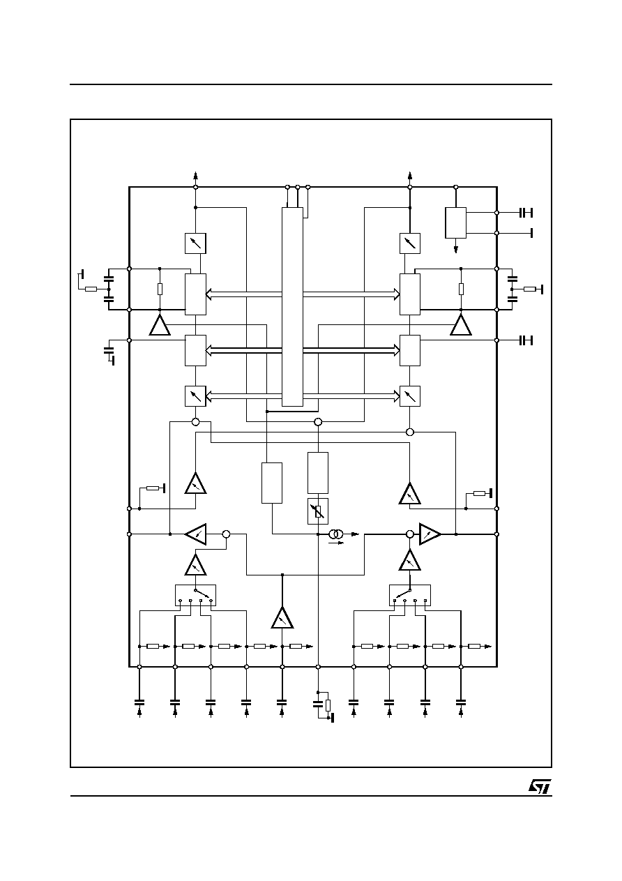
The TDA7468D is a volume tone (bass and
treble) balance (Left/Right) processor for quality
audio applications in Hi-Fi systems.
Selectable input gain is provided. Control of all
the functions is accomplished by serial bus.
The AC signal setting is obtained by resistor net-
works and switches combined with operational
amplifiers.
Thanks to the used BIPOLAR/CMOS Technology,
Low Distortion, Low Noise and DC stepping are
obtained
February 2002
ORDERING NUMBER: TDA7468D
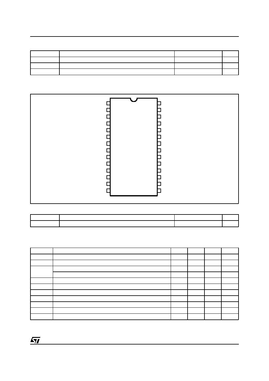
SO28
Æ
1/21

IN-R3
ALC
SUPPLY
V
S
GND
CREF
TREBLE-L
MUX-L
IS-L
D99AU1058A
I2
C BUS DECODER + LATCHES
SCL
SDA
OUT-L
OUT-R
+
+
+
TREBLE-R
MUX-R
BASSI-R
IS-R
BASSO-R
50K
50K
50K
TREBLE
gm
gm
buffer gain:
0 to 14dB gain
/ 2dB step
63dB att.
/1dB step
+ 6dB gain
-14 to +14dB
/2dB step
-14 to +14dB
/2dB step
-14 to +14dB
/2dB step
-14 to +14dB
/2dB step
-24 att.
/8dB step
-24 att.
/8dB step
63dB att.
/1dB step
+ 6dB gain
0dB
6dB
9dB
12dB
0dB
6dB
9dB
12dB
non-inverting
inverting
VARIABLE
MIX
VARIABLE
MIX
non-inverting
inverting
0dB, 6dB
10dB, 14dB
INPUT
SELECT
TREBLE
BASS
BASS
BASS_ALC
CONTROL
HALF_WAVE
RECTIFIER
IN-R2
IN-R4
23
24
25
26
2
16
50K
50K
V
REF
BASSO-L
BASSI-L
IN-R1
50K
50K
IN-L2
50K
buffer gain:
0 to 14dB gain
/ 2dB step
INPUT
SELECT
IN-L3
IN-L1
3
4
5
6
78
9
1
0
1
1
2
8
2
7
1
DGND
13
12
15
14
17
18
19
20
21
22
MIC-MIX
50K
50K
IN-L4
50K
+
+
BLOCK DIAGRAM
TDA7468D
2/21
IN4_L
MUX_L
IS_L
TREBLE_L
BASSI_L
OUT_L
BASSO_L
DGND
SCL
1
3
2
4
5
6
7
8
9
SDA
ALC
OUT_R
BASSI_R
BASSO_R
IS_R
MUX_R
TREBLE_R
IN4_R
23
22
21
20
19
17
18
16
15
D99AU1057
10
11
12
13
14
28
27
26
25
24
V
S
MIC
IN1_L
IN2_L
IN3_L
IN3_R
IN2_R
IN1_R
CREF
GND
PIN CONNECTION
ABSOLUTE MAXIMUM RATINGS
Symbol
Parameter
Value
Unit
V
S
Operating Supply Voltage
10.5
V
T
amb
Operating Ambient Temperature
-10 to 85
∞
C
T
stg
Storage Temperature Range
-55 to 150
∞
C
THERMAL DATA
Symbol
Parameter
Value
Unit
R
th j-pin
Thermal Resistance Junction-pins
85
∞
C/W
QUICK REFERENCE DATA
Symbol
Parameter
Min.
Typ.
Max.
Unit
V
S
Supply Voltage
5
9
10
V
V
CL
Max. input signal handling
2
V
rms
THD
Total Harmonic Distortion V
I
= 1V
rms
f = 1KHz
0.01
%
Total Harmonic Distortion V
I
= 0.1V
rms
f = 1KHz
0.1
%
S/N
Signal to Noise Ratio V
out
= 1V
rms
(0dB)
100
dB
S
C
Channel Separation f = 1KHz
90
dB
Input Gain (2dB step)
0
14
dB
Volume Control (1dB step)
-87
0
dB
Treble Control (2dB step)
-14
+14
dB
Bass Control (2dB step)
-14
+14
dB
Mute Attenuation
86
dB
TDA7468D
3/21

ELECTRICAL CHARACTERISTICS (refer to the test circuit T
amb
= 25∞C, V
S
= 9V, f = 1KHz
all controls flat (G = 0dB), unless otherwise specified)
Symbol
Parameter
Test Condition
Min.
Typ.
Max.
Unit
SUPPLY
V
S
Supply Voltage
5
9
10
V
I
S
Supply Current
9
mA
SVR
Ripple Rejection
60
90
dB
INPUT STAGE
R
IN
Input Resistance
35
50
65
K
V
CL
Clipping Level
THD = 0.3%
2
2.5
V
rms
S
IN
Input Separation
80
100
dB
G
inmin
Minimum Input Gain
-1
0
1
dB
G
inmax
Maximum Input Gain
14
dB
G
step
Step Resolution
2
dB
MIC
R
IN
Input Resistance
35
50
65
K
G
mic1
Mic Input Gain 1
14
dB
G
mic2
Mic Input Gain 2
10
dB
G
mic3
Mic Input Gain 3
6
dB
G
min4
Mic Input Gain 4
0
dB
MIX
mic
Mixing Rate
50
%
SURROUND
R
in
Input Resistance
35
50
65
K
G
inmin
Minimum Input Gain
-1
0
1
dB
G
inmax
Maximum Input Gain
12
dB
G
inV
Inverting Gain
-1
Mix
min
Minimum Mixing Rate
0
%
Mix
max
Maximum Mixing Rate
100
%
Crosstalk
Crosstalk of Mux Output to
100% IS
40
dB
G
buffer
Buffer Gain
6
dB
VOLUME CONTROL
C
RANGE1
Vol 1 Control Range
63
dB
A
VMAX1
Vol 1 Max. Attenuation
61
63
65
dB
A
STEP1
Vol 1 Step Resolution
0.5
1
1.5
dB
Match1
Matching
TBD
dB
C
RANGE2
Vol 2 Control Range
24
dB
A
VMAX2
Vol 2 Max. Attenuation
22
24
26
dB
A
STEP2
Vol 2 Step Resolution
7
8
9
dB
Match2
Matching
TBD
dB
A
VMAX1
+
A
VMAX2
Vol 1 + Vol 2 Max Attenuation
84
dB
BASS CONTROL
Gb
Control Range
Max. Boost/cut
+12.0
+14.0
+16.0
dB
B
STEP
Step Resolution
1
2
3
dB
R
B
Internal Feedback Resistance
33
44
55
K
TDA7468D
4/21
ELECTRICAL CHARACTERISTICS (continued.)
Symbol
Parameter
Test Condition
Min.
Typ.
Max.
Unit
BASS ALC CONTROL
R
attack1
Attack Time Resistor 1
12.5
K
R
attack2
Attack Time Resistor 2
25
K
R
attack3
Attack Time Resistor 3
50
K
R
attack4
Attack Time Resistor 4
100
K
Thresh1
Threshold 1
700
mV
rms
Thresh2
Threshold 2
485
mV
rms
Thresh3
Threshold 3
320
mV
rms
Thresh4
Threshold 4
170
mV
rms
TREBLE CONTROL
Gt
Control Range
Max. Boost/cut
+13.0
+14.0
+15.0
dB
T
STEP
Step Resolution
1
2
3
dB
R
t
Internal Resistance
25
K
AUDIO OUTPUTS
V
OCL
Clipping Level
THD = 0.3%
2
2.5
V
rms
R
L
Output Load Resistance
2
K
V
OUT
DC Voltage Level
4.5
V
GENERAL
E
NO
Output Noise
BW = 20Hz to 20KHz;
All gains 0dB;
output muted
flat
5
10
15
µ
V
µ
V
S/N
Signal to Noise Ratio
All gains 0dB; V
O
= 1V
rms ;
100
dB
S
C
Channel Separation Left/Right
90
dB
d
Distortion
A
V
= 0; V
I
= 0.1V
rms
;
0.1
%
A
V
= 0; V
I
= 1V
rms
;
0.01
%
S
C
Channel Separation left/right
90
dB
Total Tracking Error
0
1
dB
BUS INPUT
V
IL
Input Low Voltage
1
V
V
IH
Input High Voltage
2.5
V
I
IN
Input Current
V
IN
= 0.4V
-5
5
µ
A
V
O
Output Voltage (ACK)
I
O
= 1.6mA
0.4
0.8
V
TDA7468D
5/21
IN-R3
ALC
0.47
µ
F
0.47
µ
F
0.47
µ
F
SUPPLY
V
S
GND
CREF
TREBLE-L
MUX-L
IS-L
D99AU1059A
I2
C BUS DECODER + LATCHES
SCL
SDA
OUT-L
OUT-R
10
µ
F
+
+
+
TREBLE-R
MUX-R
BASSI-R
IS-R
3.3nF
100nF
100nF
5.6K
BASSO-R
50K
50K
50K
1M
TREBLE
gm
gm
buffer gain:
0 to 14dB gain
/ 2dB step
63dB att.
/1dB step
+ 6dB gain
-14 to +14dB
/2dB step
-14 to +14dB
/2dB step
-14 to +14dB
/2dB step
-14 to +14dB
/2dB step
-24 att.
/8dB step
-24 att.
/8dB step
63dB att.
/1dB step
+ 6dB gain
0dB
6dB
9dB
12dB
0dB
6dB
9dB
12dB
non-inverting
inverting
VARIABLE
MIX
VARIABLE
MIX
non-inverting
inverting
0dB, 6dB
10dB, 14dB
INPUT
SELECT
TREBLE
BASS
BASS
BASS_ALC
CONTROL
HALF_WAVE
RECTIFIER
IN-R2
IN-R4
23
24
25
26
2
16
0.47
µ
F
50K
50K
V
REF
BASSO-L
BASSI-L
0.47
µ
F
0.47
µ
F
IN-R1
50K
50K
IN-L2
0.47
µ
F
0.47
µ
F
50K
buffer gain:
0 to 14dB gain
/ 2dB step
INPUT
SELECT
IN-L3
IN-L1
3
4
5
6
78
9
1
0
1
1
2
8
2
7
1
DGND
13
12
15
14
17
18
19
20
21
22
0.47
µ
F
MIC-MIX
50K
50K
0.47
µ
F
IN-L4
50K
+
+
TEST CIRCUIT
TDA7468D
6/21
APPLICATION SUGGESTIONS
The first and the last stages are volume control
blocks. The control range is 0 to -63dB (mute)
with 1dB step resolution for this first one, 0 to
24dB (mute) with 8dB step resolution for the last
one..
The very high resolution allows the implementation
of systems free from any noisy acoustical effect.
The TDA7468D audioprocessor provides 2 bands
tones control.
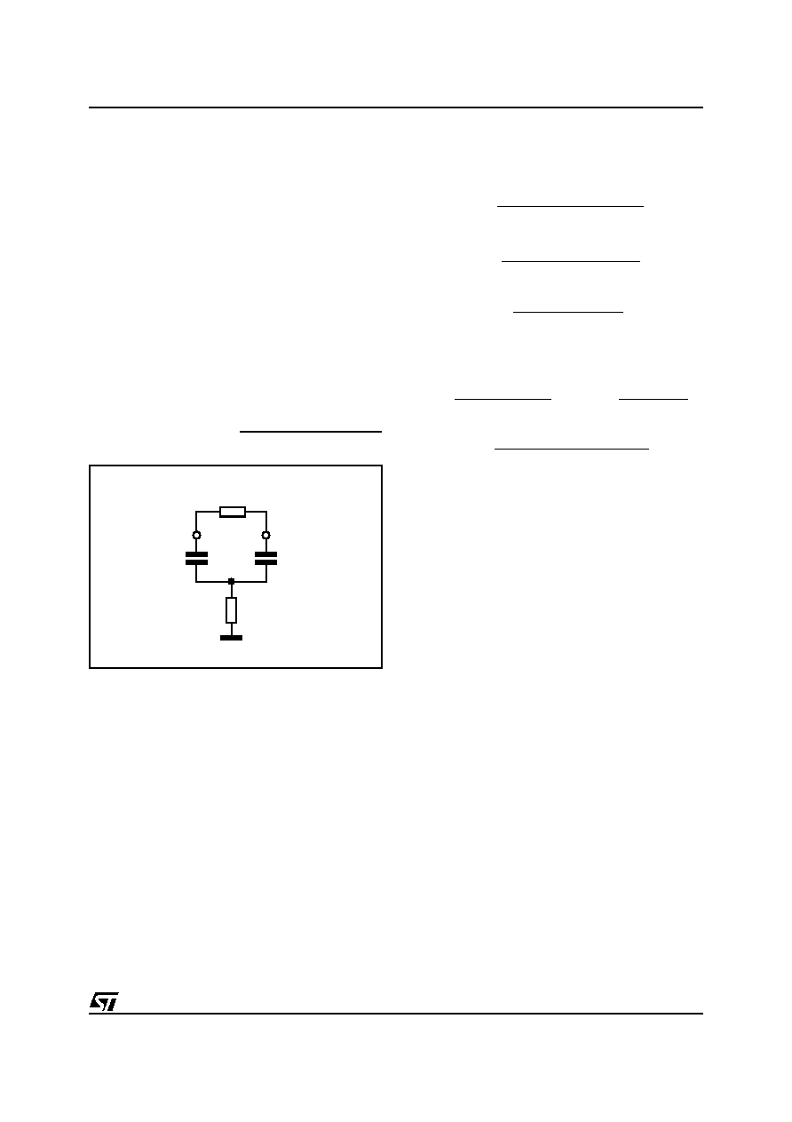
Bass, Stages
The Bass cell has an internal resistor Ri = 44K
typical.
Several filter types can be implemented, connect-
ing external components to the Bass IN and OUT
pins.
The fig.1 refers to basic T Type Bandpass Filter
starting from the filter component values (R1 in-
ternal and R2,C1,C2 external) the centre fre-
quency Fc, the gain Av at max. boost and the fil-
ter Q factor are computed as follows:
F
C
=
1
2
R1
R2
C1
C2
A
V
=
R2 C2
+
R2 C1
+
Ri C1
R2 C1
+
R2 C2
Q
=
R1
R2
C1
C2
R2 C1
+
R2 C2
Viceversa, once Fc, Av, and Ri internal value are
fixed, the external components values will be:
C1
=
A
V
-
1
2
F
C
R
i
Q
C2
=
Q
2
C1
A
V
-
1
-
Q
2
R2
=
A
V
-
1
-
Q
2
2
C1
F
C
(
A
V
-
1
)
Q
Treble Stage
The treble stage is a high pass filter whose time
constant is fixed by an internal resistor (25K
typical) and an external capacitor connected be-
tween treble pins and ground
CREF
The suggested 10
µ
F reference capacitor (CREF)
value can be reduced to 4.7
µ
F if the application
requires faster power ON.
Ri internal
C
2
OUT
IN
C
1
R
2
D95AU313
Figure 1.
TDA7468D
7/21

I
2
C BUS INTERFACE
Data transmission from microprocessor to the
TDA7468D and vice versa takes place through
the 2 wires I
2
C BUS interface, consisting of the
two lines SDA and SCL (pull-up resistors to posi-
tive supply voltage must be connected).
Data Validity
As shown in fig. 2, the data on the SDA line must
be stable during the high period of the clock. The
HIGH and LOW state of the data line can only
change when the clock signal on the SCL line is
LOW.
Start and Stop Conditions
As shown in fig.3 a start condition is a HIGH to
LOW transition of the SDA line while SCL is
HIGH. The stop condition is a LOW to HIGH tran-
sition of the SDA line while SCL is HIGH.
Byte Format
Every byte transferred on the SDA line must con-
tain 8 bits. Each byte must be followed by an ac-
knowledge bit. The MSB is transferred first.
Acknowledge
The master (
µ
P) puts a restive HIGH level on the
SDA line during the acknowledge clock pulse (see
fig. 4). The peripheral (audio processor) that ac-
knowledges has to pull-down (LOW) the SDA line
during this clock pulse.
The audio processor which has been addressed
has to generate an acknowledge after the recep-
tion of each byte, otherwise the SDA line remains
at the HIGH level during the ninth clock pulse
time. In this case the master transmitter can gen-
erate the STOP information in order to abort the
transfer.
Transmission without Acknowledge
Avoiding to detect the acknowledge of the audio
processor, the
µ
P can use a simpler transmission:
simply it waits one clock without checking the
slave acknowledging, and sends the new data.
This approach of course is less protected from
misworking.
Figure 2: Data Validity on the I
2
CBUS
Figure 3: Timing Diagram of I
2
CBUS
Figure 4: Acknowledge on the I
2
CBUS
TDA7468D
8/21

SOFTWARE SPECIFICATION
Interface Protocol
The interface protocol comprises:
A start condition (S)
A chip address byte, containing the TDA7468D
address
A subaddress bytes
A sequence of data (N byte + acknowledge)
A stop condition (P)
ACK = Acknowledge
S = Start
P = Stop
A = Address
B = Auto Increment
S
1
0
0
0
1
0
0
0
ACK
ACK
DATA
ACK
P
MSB
LSB
MSB
LSB
MSB
LSB
CHIP ADDRESS
D96AU420
X
DATA
SUBADDRESS
DATA 1 to DATA n
X
X
B
EXAMPLES
No Incremental Bus
The TDA7468D receives a start condition, the
correct chip address, a subaddress with the B = 0
(no incremental bus), N-data (all these data con-
cern the subaddress selected), a stop condition.
S
1
0
0
0
1
0
0
0
ACK
ACK
DATA
ACK
P
MSB
LSB
MSB
LSB
MSB
LSB
CHIP ADDRESS
D96AU421
X
D3
SUBADDRESS
DATA
X
X
0
D2 D1 D0
Incremental Bus
The TDA7468D receive a start conditions, the
correct chip address, a subaddress with the B = 1
(incremental bus): now it is in a loop condition
with an autoincrease of the subaddress whereas
SUBADDRESS from "XXX1000" to "XXX1111" of
DATA are ignored.
The DATA 1 concern the subaddress sent, and
the DATA 2 concern the subaddress sent plus
one in the loop etc, and at the end it receivers the
stop condition.
S
1
0
0
0
1
0
0
0
ACK
ACK
DATA
ACK
P
MSB
LSB
MSB
LSB
MSB
LSB
CHIP ADDRESS
D96AU422
X
D3
SUBADDRESS
DATA 1 to DATA n
X
X
1
D2 D1 D0
TDA7468D
9/21
POWER ON RESET CONDITION
MSB
LSB
D7
D6
D5
D4
D3
D2
D1
D0
1
1
1
1
1
1
1
0
DATA BYTES
Address = (HEX) 10001000.
FUNCTION SELECTION: First byte (subaddress)
MSB
LSB
SUBADDRESS
D7
D6
D5
D4
D3
D2
D1
D0
X
X
X
B
0
0
0
0
INPUT SELECT & MIC
X
X
X
B
0
0
0
1
INPUT GAIN
X
X
X
B
0
0
1
0
SURROUND
X
X
X
B
0
0
1
1
VOLUME LEFT
X
X
X
B
0
1
0
0
VOLUME RIGHT
X
X
X
B
0
1
0
1
TREBLE & BASS
X
X
X
B
0
1
1
0
OUTPUT
X
X
X
B
0
1
1
1
BASS ALC
B = 1: INCREMENTAL BUS; ACTIVE
B = 0: NO INCREMENTAL BUS
X = INDIFFERENT 0/1
INPUT SELECTION & MIC
MSB
LSB
D7
D6
D5
D4
D3
D2
D1
D0
INPUT SELECT
0
0
0
IN1
0
0
1
IN2
0
1
0
IN3
0
1
1
IN4
MUTE (IN5)
1
ON (IN5)
0
OFF
MIC
0
0
Gain: 14dB
0
1
Gain: 10dB
1
0
Gain: 6dB
1
1
Gain: 0dB
1
OFF
0
ON
TDA7468D
10/21
DATA BYTES (continued)
INPUT GAIN SELECTION
MSB
LSB
INPUT GAIN
D7
D6
D5
D4
D3
D2
D1
D0
2dB STEPS
0
0
0
0dB
0
0
1
2dB
0
1
0
4dB
0
1
1
6dB
1
0
0
8dB
1
0
1
10dB
1
1
0
12dB
1
1
1
14dB
GAIN = 0 to 30dB
SURROUND
MSB
LSB
SURROUND
D7
D6
D5
D4
D3
D2
D1
D0
SURROUND MODE
1
ON
0
OFF
GAIN
0
0
0dB
0
1
6dB
1
0
9dB
1
1
12dB
MIXING
0
0
0
inverting : 100%
0
0
1
inverting :50%
0
1
0
inverting : 25%
0
1
1
0%
1
0
0
non-inverting : 100%
1
0
1
non-inverting : 75%
1
1
0
non-inverting : 50%
1
1
1
mute
BUFFER GAIN
1
0
0
6dB
TDA7468D
11/21
VOLUME
MSB
LSB
VOLUME
D7
D6
D5
D4
D3
D2
D1
D0
1dB STEPS
0
0
0
0dB
0
0
1
-1dB
0
1
0
-2dB
0
1
1
-3dB
1
0
0
-4dB
1
0
1
-5dB
1
1
0
-6dB
1
1
1
-7dB
8dB STEPS
0
0
0
0dB
0
0
1
-8dB
0
1
0
-16dB
0
1
1
-24dB
1
0
0
-32dB
1
0
1
-40dB
1
1
0
-48dB
1
1
1
-56dB
VOLUME 2
0
0
0dB
0
1
-8dB
1
0
-16dB
1
1
-24dB
VOLUME = 0 to-87dB
TDA7468D
12/21
VOLUME setting 1
Target Volume
(dB)
Volume1 1dB step (dB)
Volume1 8dB step (dB)
Volume2 8dB step (dB)
0
-1
-2
-3
-4
-5
-6
-7
0
-1
-2
-3
-4
-5
-6
-7
0
0
-8
-9
-10
-11
-12
-13
-14
-15
0
-1
-2
-3
-4
-5
-6
-7
-8
0
-16
-17
-18
-19
-20
-21
-22
-23
0
-1
-2
-3
-4
-5
-6
-7
-16
0
-24
-25
-26
-27
-28
-29
-30
-31
0
-1
-2
-3
-4
-5
-6
-7
-24
0
-32
-33
-34
-35
-36
-37
-38
-39
0
-1
-2
-3
-4
-5
-6
-7
-32
0
-40
-41
-42
-43
-44
-45
-46
-47
0
-1
-2
-3
-4
-5
-6
-7
-40
0
-48
-49
-50
-51
-52
-53
-54
-55
0
-1
-2
-3
-4
-5
-6
-7
-48
0
TDA7468D
13/21

VOLUME setting 1 (continued)
Target Volume
(dB)
Volume1 1dB step (dB)
Volume1 8dB step (dB)
Volume2 8dB step (dB)
-56
-57
-58
-59
-60
-61
-62
-63
0
-1
-2
-3
-4
-5
-6
-7
-56
0
-64
-65
-66
-67
-68
-69
-70
-71
0
-1
-2
-3
-4
-5
-6
-7
-56
8
-72
-73
-74
-75
-76
-77
-78
-79
0
-1
-2
-3
-4
-5
-6
-7
-56
-16
-80
-81
-82
-83
-84
-85
-86
-87
0
-1
-2
-3
-4
-5
-6
-7
-56
-24
TDA7468D
14/21

VOLUME setting 2
Target Volume
(dB)
Volume1 1dB step (dB)
Volume1 8dB step (dB)
Volume2 8dB step (dB)
0
-1
-2
-3
-4
-5
-6
-7
0
-1
-2
-3
-4
-5
-6
-7
0
0
-8
-9
-10
-11
-12
-13
-14
-15
0
-1
-2
-3
-4
-5
-6
-7
-8
0
-16
-17
-18
-19
-20
-21
-22
-23
0
-1
-2
-3
-4
-5
-6
-7
-16
0
-24
-25
-26
-27
-28
-29
-30
-31
0
-1
-2
-3
-4
-5
-6
-7
-16
-8
-32
-33
-34
-35
-36
-37
-38
-39
0
-1
-2
-3
-4
-5
-6
-7
-16
-16
-40
-41
-42
-43
-44
-45
-46
-47
0
-1
-2
-3
-4
-5
-6
-7
-16
-24
-48
-49
-50
-51
-52
-53
-54
-55
0
-1
-2
-3
-4
-5
-6
-7
-24
-24
TDA7468D
15/21

VOLUME setting 2 (continued)
Target Volume
(dB)
Volume1 1dB step (dB)
Volume1 8dB step (dB)
Volume2 8dB step (dB)
-56
-57
-58
-59
-60
-61
-62
-63
0
-1
-2
-3
-4
-5
-6
-7
-32
-24
-64
-65
-66
-67
-68
-69
-70
-71
0
-1
-2
-3
-4
-5
-6
-7
-40
-24
-72
-73
-74
-75
-76
-77
-78
-79
0
-1
-2
-3
-4
-5
-6
-7
-48
-24
-80
-81
-82
-83
-84
-85
-86
-87
0
-1
-2
-3
-4
-5
-6
-7
-56
-24
TDA7468D
16/21

TREBLE & BASS SELECTION
MSB
LSB
D7
D6
D5
D4
D3
D2
D1
D0
TREBLE
0
0
0
0
-14dB
0
0
0
1
-12dB
0
0
1
0
-10dB
0
0
1
1
-8dB
0
1
0
0
-6dB
0
1
0
1
-4dB
0
1
1
0
-2dB
0
1
1
1
0dB
1
0
0
0
14dB
1
0
0
1
12dB
1
0
1
0
10dB
1
0
1
1
8dB
1
1
0
0
6dB
1
1
0
1
4dB
1
1
1
0
2dB
1
1
1
1
0dB
BASS (*)
0
0
0
0
-14dB
0
0
0
1
-12dB
0
0
1
0
-10dB
0
0
1
1
-8dB
0
1
0
0
-6dB
0
1
0
1
-4dB
0
1
1
0
-2dB
0
1
1
1
0dB
1
0
0
0
14dB
1
0
0
1
12dB
1
0
1
0
10dB
1
0
1
1
8dB
1
1
0
0
6dB
1
1
0
1
4dB
1
1
1
0
2dB
1
1
1
1
0dB
(*) When BASS is programmed in the range -14dB/0dB, ALC is automatically switched to "OFF".
TDA7468D
17/21
DATA BYTES (continued)
OUTPUT
MSB
LSB
D7
D6
D5
D4
D3
D2
D1
D0
MUTE
0
ON
1
OFF
BASS ALC
MSB
LSB
BASS ALC
D7
D6
D5
D4
D3
D2
D1
D0
ALC Mode
1
ON
0
OFF
Detector
1
ON
0
OFF
Release Current Circuit
1
ON
0
OFF
Attack Time Resistor
0
0
12.5K
0
1
25K
1
0
50K
1
1
100K
Threshold
0
0
700mVrms
0
1
485mVrms
1
0
320mVrms
1
1
170mVrms
Attack Mode
0
MODE 1: Fixed Resistor
1
MODE 2: Adaptive
0.1
1
0.01
0.1
1
V
O
(V
RMS
)
V
IN
(V
RMS
)
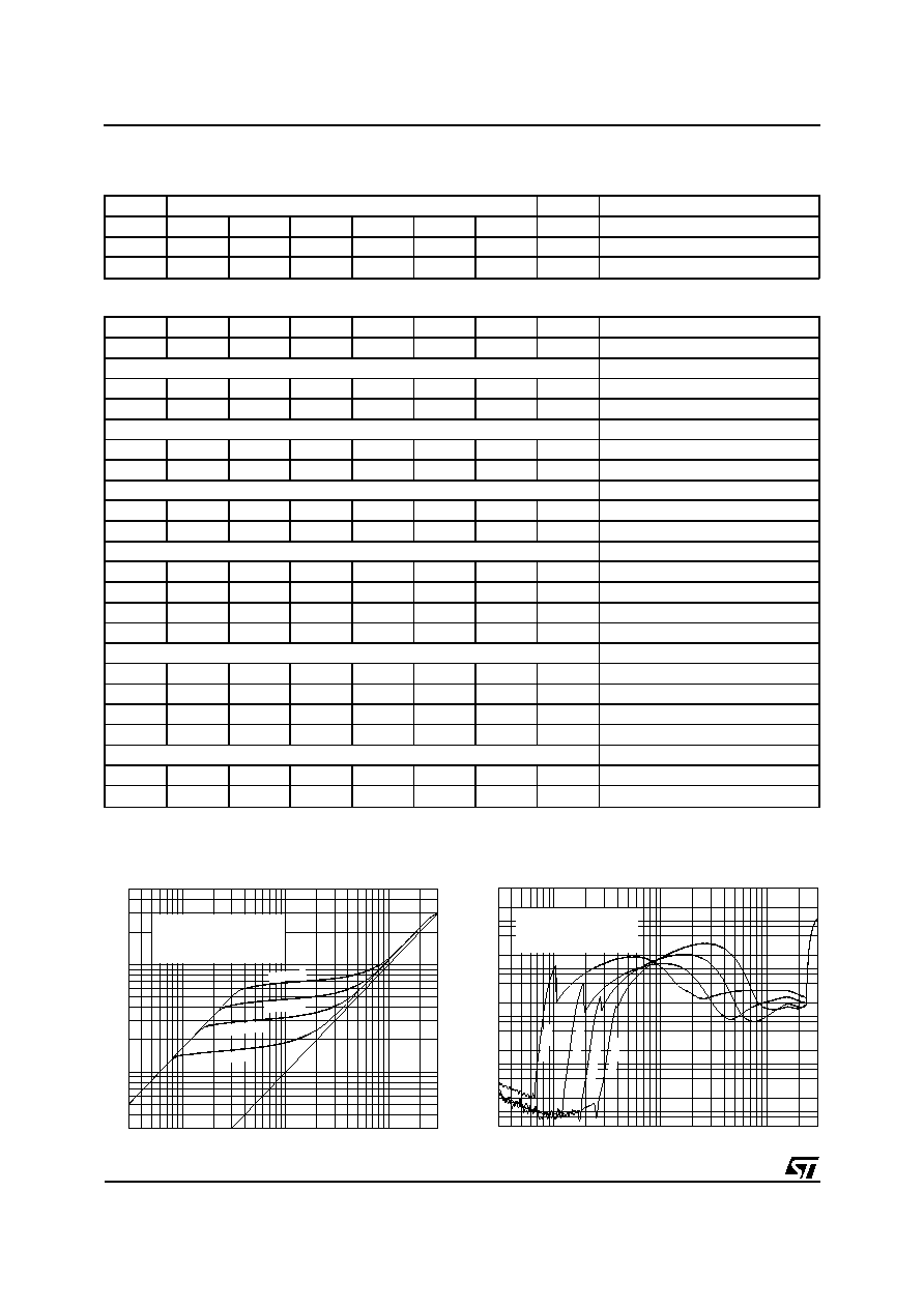
D00AU1100
Supply Voltage : 9.0V
Frequency : 60Hz
Bassfilter : 60Hz/28dB boost
Internal release circuit : ON
Attack mode : 12.5kohm, mode2(adaptive)
Threshold1
Threshold2
Threshold4
Threshold3
BASS ALC : Threshold curve
0.001
0.01
0.1
1
10
0.01
0.1
1
V
IN
(V
RMS
)
THD
[%]
Threshold4
Threshold3
Threshold2
Threshold1
Supply Voltage : 9.0V
Frequency : 60Hz
Bassfilter : 60Hz/28dB boost
Internal release circuit : ON
Attack mode : 12.5kohm, mode2(adaptive)
D99AU1101A
BASS ALC : THD
TDA7468D
18/21

25K
V
S
D99AU1094
20
µ
A
GND
PINS: TREBLE_L, TREBLE_R
20
µ
A
V
S
D99AU1095
GND
PINS: SCL, SDA
20
µ
A
V
S
50K
Vref
D99AU1092
GND
PINS: IN1_L, IN1_R, IN2_L, IN2_R, IN3_L,
IN3_R, IN4_L, IN4 _R, IS_L, IS_R,
MIC
10
V
S
D99AU1093
20
µ
A
GND
PINS: OUT_L, OUT_R, IMUX_L, MUX_R,
45K
V
S
D99AU1096
20
µ
A
BASSO-L,BASSO-R
GND
PINS: BASSI_L, BASSI_R
45K
V
S
D99AU1097
20
µ
A
BASSI-L,BASSI-R
GND
PINS: BASSO_L, BASSO_R
100K
V
S
D99AU1098
20
µ
A
GND
PIN: ALC
25K
25K
GND
V
S
D99AU1099
20
µ
A
PIN: CREF
IC1
TDA7468D
19/21
SO28
DIM.
mm
inch
MIN.
TYP.
MAX.
MIN.
TYP.
MAX.
A
2.65
0.104
a1
0.1
0.3
0.004
0.012
b
0.35
0.49
0.014
0.019
b1
0.23
0.32
0.009
0.013
C
0.5
0.020
c1
45
∞
(typ.)
D
17.7
18.1
0.697
0.713
E
10
10.65
0.394
0.419
e
1.27
0.050
e3
16.51
0.65
F
7.4
7.6
0.291
0.299
L
0.4
1.27
0.016
0.050
S
8
∞
(max.)
OUTLINE AND
MECHANICAL DATA
TDA7468D
20/21

Information furnished is believed to be accurate and reliable. However, STMicroelectronics assumes no responsibility for the consequences
of use of such information nor for any infringement of patents or other rights of third parties which may result from its use. No license is
granted by implication or otherwise under any patent or patent rights of STMicroelectronics. Specification mentioned in this publication are
subject to change without notice. This publication supersedes and replaces all information previously supplied. STMicroelectronics products
are not authorized for use as critical components in life support devices or systems without express written approval of STMicroelectronics.
The ST logo is a registered trademark of STMicroelectronics
© 2002 STMicroelectronics ≠ Printed in Italy ≠ All Rights Reserved
STMicroelectronics GROUP OF COMPANIES
Australia - Brazil - Canada - China - Finland - France - Germany - Hong Kong - India - Israel - Italy - Japan - Malaysia - Malta - Morocco -
Singapore - Spain - Sweden - Switzerland - United Kingdom - United States.
http://www.st.com
TDA7468D
21/21