 | ÐлекÑÑоннÑй компоненÑ: TDA7478D | СкаÑаÑÑ:  PDF PDF  ZIP ZIP |
Äîêóìåíòàöèÿ è îïèñàíèÿ www.docs.chipfind.ru
1/8
TDA7478
November 2004
1
FEATURES
VERY HIGH RDS DEMODULATION QUALITY
WITH IMPROVED DIGITAL SIGNAL
PROCESSING
HIGH PERFORMANCE, 57KHz BANDPASS
FILTER (8th ORDER)
FILTER ADJUSTMENT FREE AND WITHOUT
EXTERNAL COMPONENTS
PURELY DIGITAL RDS DEMODULATION
WITHOUT EXTERNAL COMPONENTS
RDS SIGNAL QUALITY OUTPUT
4.332MHz CRYSTAL OSCILLATOR(8.664MHz
OPTIONAL)
LOW NOISE CMOS TECHNOLOGY
LOW RADIATION
2
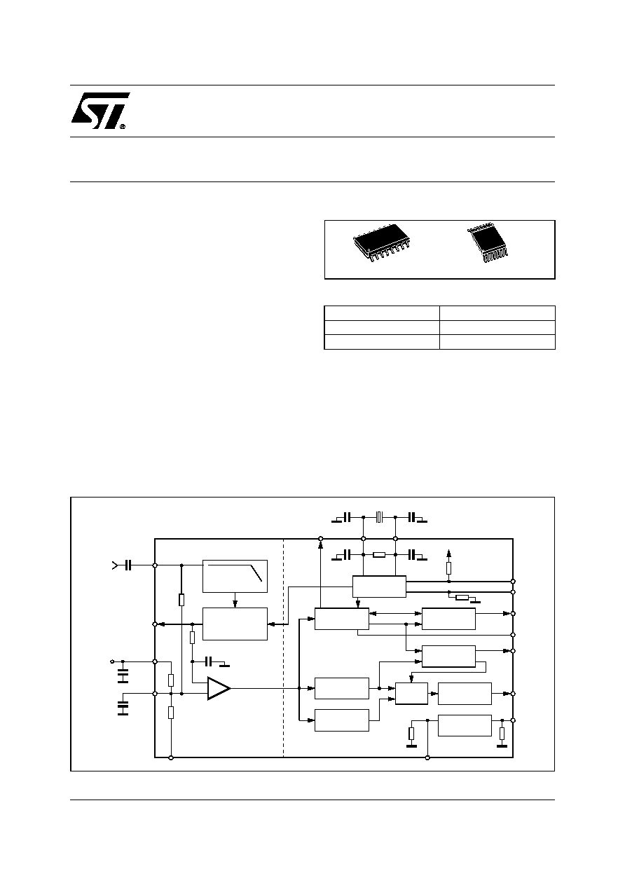
DESCRIPTION
The TDA7478 recovers the additional inaudible RDS
information which is transmitted by FM radio broad-
casting stations and operates in accordance with the
EBU (European Broadcasting Union) specifications.
The device is made up of two sections: a cascaded
antialiasing + switched capacitors 8
th
bandpass filter
for precise RDS band selection and a demodulating
section that performs the extraction od RDS data
stream (RDDA) and clock (RDCL), to be further pro-
cessed by a suitable RDS decoder.
Output for RDS signal quality is also present.
SINGLE CHIP RDS DEMODULATOR
Figure 2. Block Diagram
2nd ORDER
ANTIALIASING
FILTER
8th ORDER
SC-BANDPASS
FILTER
MPX
4
270pF
-
+
8
FILOUT
12
V
S
3
VREF
100nF
10
µF
OSCILLATOR &
DIVIDER
57KHz PLL
POLARITY
BIPHASE DEC.
INTEGRAL
BIPHASE DEC.
1187.5Hz
PLL
MUX
0
1
DIFF. DECODER
TEST LOGIC
QUAL DET.
6
GND
11
EXTRES
14
13
5
9
16
7
1
D03AU1490
TM
10
RDDA
2
QUAL
N.U.
RDCL
FSEL
OSEL
OSCOUT
OSCIN
4.332MHz
C2 47pF
C1 27pF
15
T57
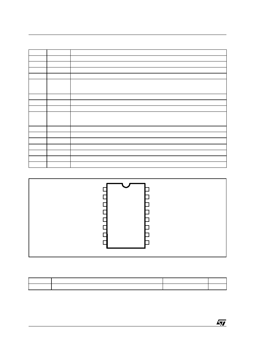
Figure 1. Packages
Table 1. Order Codes
Part Number
Package
TDA7478D
SO16
E-TDA7478AD
TSSOP16
SO16
TSSOP16
Rev. 2
TDA7478
2/8
Table 2. Pin Description
Figure 3. Pin Connection (Top view)
Table 3. Thermal Data
No pin
Name
Description
1
QUAL
Output for signal quality indication (High = good)
2
RDDA
RDS data output
3
VREF
Reference voltage
4
MPX
RDS input signal
5
OSEL
Oscillator selector pin:
- open, closed to V
S
= quartz oscillator
- closed to GND=external driven
6
GND
Ground
7
N.U.
Not Used (to be left open)
8
FILOUT
Filter output
9
FSEL
Frequency selector pin:
- open = 4.332MHz
- closed to VS = 8.664MHz
10
TM
Test mode pin: - open = normal operation - closed to VS = testmode
11
EXTRES
Reset pin: - open=run mode - closed to VS = reset condition
12
V
S
Supply voltage
13
OSCIN
Oscillator input
14
OSCOUT
Oscillator output
15
T57
Testing output pin: 57kHz clock output
16
RDCL
RDS clock output 1187.5Hz
Symbol
Description
Value
Unit
R
th j-case
Thermal Resistance Junction-case Max.
200
°C/W
QUAL
RDDA
VREF
MPX
OSEL
N.U.
GND
1
3
2
4
5
6
7
TM
V
S
EXTRES
OSCIN
OSCOUT
T57
RDCL
16
15
14
13
12
10
11
D97AU752A
FILOUT
8
FSEL
9
3/8
TDA7478
Table 4. Absolute Maximum Ratings
(1) The 3rd harmonic (57kHz) must be less than -40dB with respect to the input signal plus gain.
Symbol
Parameter
Value
Unit
V
S
Supply Voltage
-0.3 to 7
V
T
op
Operating Temperature Range
-40 to 85
°C
T
stg
Storage Temperature
-55 to 150
°C
Table 5. Electrical Characteristcs
(T
amb
= 25°C, V
S
= 5V, unless otherwise specified)
Symbol
Parameter
Test Condition
Min.
Typ.
Max.
Unit
V
S
Supply voltage
4.5
5
5.5
V
I
S
Supply current
7.5
12.0
mA
FILTER
f
C
Center frequency
56.6
57
57.4
kHz
BW
3dB Bandwidth
2.5
3
3.5
kHz
G
Gain
f = 57kHz
17
20
23
dB
A
Attenuation
f ± 4kHz
22
dB
f = 38kHz
60
dB
f = 67kHz
45
dB
R
I
Input impedance of MPX
120
K
R
L
Load impedance on FILOUT
1
M
S/N
Signal to noise ratio
V
IN
= 3mVRMS
30
40
dB
V
IN
MPX input signal
f = 19kHz; T3
40dB
(1)
f = 57kHz (RDS)
1000
50
mV
RMS
mV
RMS
S
RDS
RDS Detection Sensitivity
1
mVrms
S
ARI
ARI Detection Sensitivity
3
mVrms
V
REF
Reference
V
S
/2
V
DEMODULATOR
Input pins (EXTRES, FSEL, TM)
all with internal pull down resistor
Input pin (OSEL)
with internal pull up resistor
I
PD
Input Current
V
IN
= 5V (pull-down input)
15
30
µA
I
PU
Input Current
V
IN
= 0V (pull-up input)
-25
-10
µA
V
IH
Input voltage high
0.7 · V
S
0.8 · V
S
V
VIL
Input voltage low
0.2 · V
S
0.3 · V
S
V
Output pins (RDCL, RDDA, QUAL, T57)
V
OH
Ouput voltage high
I
L
= 0.5mA
4
4.6
V
V
OL
Output voltage low
I
L
= 0.5mA
0.4
1
V
OSCILLATOR
VCLL
Input level OSCIN pin
OSEL = open circuit
1
V
VCLH
Input level OSCIN pin
OSEL = open circuit
4
V
Amplitude OSCOUT
OSEL = open circuit
4.5
V
V
PP
Amplitude OSCIN
(for external drive)
OSEL = GND, f = 4.332MHz
OSEL = GND, f = 8.664MHz
100
120
mVpp
mVpp
TDA7478
4/8
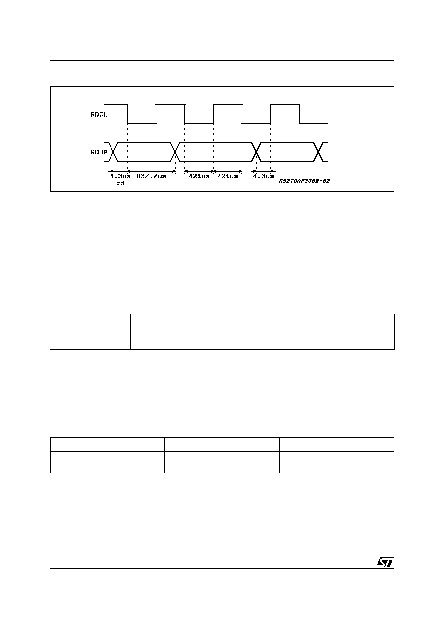
Figure 4. RDS timing diagram
3
OUTPUT TIMING
The RDS (1187.5Hz) output clock on RDCL line is synchronized to the incoming data. According to the internal
PLL lock condition data change can result on the falling or on the rising clock edge. (see Fig. 1)Whichever clock
edge is used by the decoder (rising or falling edge) the data will remain valid for 416.7
µs after the clock transi-
tion.
4
OSCILLATOR CONTROLS (FSEL, OSEL)
Two different crystal frequencies can be used. The adaption of the internal clock divider to the external crystal
is achieved via the input pin FSEL. See the following table for reference:
Table 6.
A special mode is introduced to reduce EMI. With pin OSEL connected to GND the internal oscillator is switched
off and an external sinusoidal frequency could be applied on OSCIN. The peak to peak voltage of this signal
can be reduced down to 60mV.
In this mode the frequency selection via FSEL is still active.
Suggested values of C1 and C2 are shown in the following table:
Table 7.
Crystal
FSEL (pin configuration)
4.332MHz
8.664MHz
connected to GND or open
connected to Vs
Crystal
C1
C2
4.332MHz
8.664MHz
27pF
27pF
47pF
-
CLOCK
LINE
DATA
LINE
5/8
TDA7478
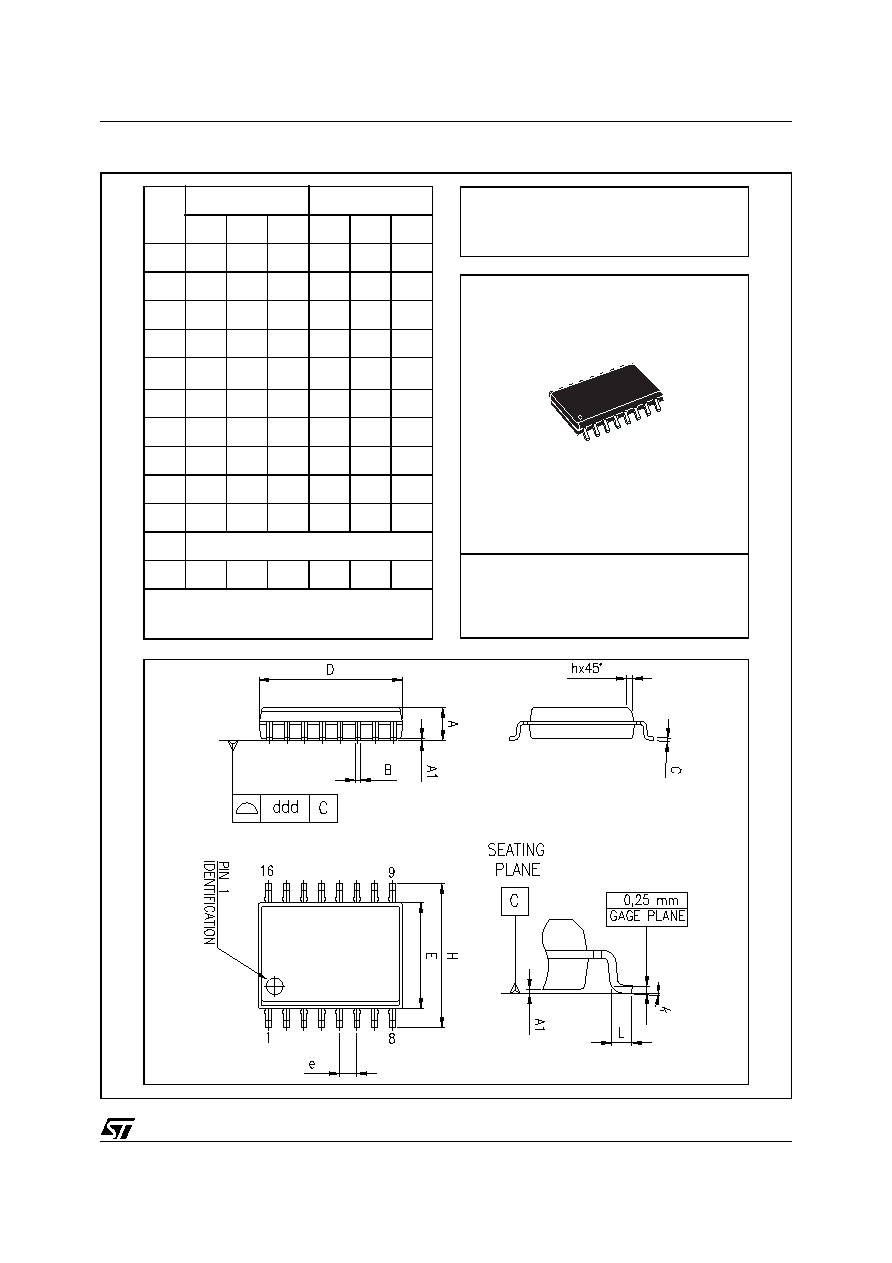
Figure 5. SO16 Mechanical Data & Package Dimensions
OUTLINE AND
MECHANICAL DATA
DIM.
mm
inch
MIN.
TYP.
MAX.
MIN.
TYP.
MAX.
A
2.35
2.65
0.093
0.104
A1
0.10
0.30
0.004
0.012
B
0.33
0.51
0.013
0.200
C
0.23
0.32
0.009
0.013
D
(1)
10.10
10.50
0.398
0.413
E
7.40
7.60
0.291
0.299
e
1.27
0.050
H
10.0
10.65
0.394
0.419
h
0.25
0.75
0.010
0.030
L
0.40
1.27
0.016
0.050
k
0° (min.), 8° (max.)
ddd
0.10
0.004
(1) "D" dimension does not include mold flash, protusions or gate
burrs. Mold flash, protusions or gate burrs shall not exceed
0.15mm per side.
SO16 (Wide)
0016021 C
Document Outline