TDA7497
10 + 10W STEREO AMPLIFIER WITH MUTE/ST-BY
PRODUCT PREVIEW
WIDE SUPPLY VOLTAGE RANGE (UP TO
±
22V ABS MAX.)
SPLIT SUPPLY
HIGH OUTPUT POWER:
10 + 10W @ THD =10%, R
L
= 8
, V
S
= +14V
NO POP AT TURN-ON/OFF
MUTE (POP FREE)
STAND-BY FEATURE (LOW I
Q
)
FEW EXTERNAL COMPONENTS
SHORT CIRCUIT PROTECTION
THERMAL OVERLOAD PROTECTION
DESCRIPTION
The TDA7497 is class AB dual Audio power am-
plifier assembled in the Multiwatt package, spe-
cially designed for high quality sound application
as Hi-Fi music centers and stereo TV sets.
This is advanced information on a new product now in development or undergoing evaluation. Details are subject to change without notice.
September 1995
Multiwatt 8
ORDERING NUMBER: TDA7497
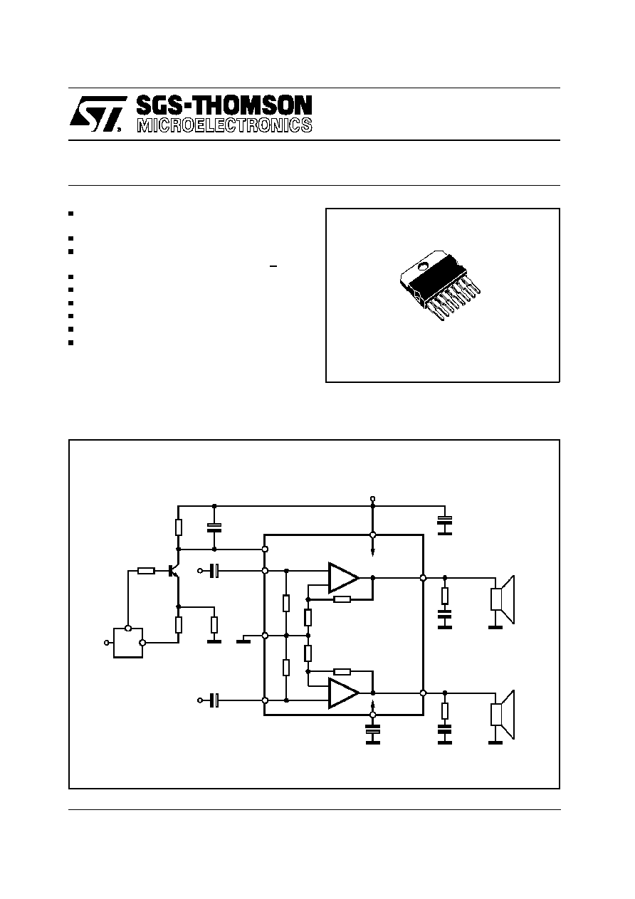
+5V
18K
15K
IN (L)
1
µ
F
15K
1
µ
F
MUTE/
ST-BY
GND
IN (R)
1
µ
F
4.7
4.7
100nF
100nF
OUT (L)
OUT (R)
1000
µ
F
1000
µ
F
+V
S
2
4
6
7
5
8
1
3
+
+
-
-
D94AU069A
RL (L)
RL (R)
+V
S
-V
S
µ
P
Figure 1: Typical Application Circuit
1/7

ABSOLUTE MAXIMUM RATINGS
Symbol
Parameter
Value
Unit
V
S
DC Supply Voltage
±
22
V
I
O
Output Peak Current (internally limited)
3
A
P
tot
Power Dissipation T
case
= 70
∞
C
12
W
T
stg
, T
j
Storage and Junction Temperature
-40 to +150
∞
C
1
2
3
4
5
6
7
D94AU096
8
IN (1)
GND
IN (2)
-V
S
MUTE/ST-BY
OUTPUT (2)
+V
S
OUTPUT (1)
Tab connected to pin 5
PIN CONNECTION (Top view)
THERMAL DATA
Symbol
Description
Value
Unit
R
th j-case
Thermal Resistance Junction-case
Max
2
∞
C/W
TDA7497
2/7

ELECTRICAL CHARACTERISTICS (Refer to the test circuit, V
S
+ 14V; R
L
= 8
; R
s
= 50
;
f = 1KHz; T
amb
= 25
∞
C, unless otherwise specified.)
Symbol
Parameter
Test Condition
Min.
Typ.
Max.
Unit
V
S
Supply Range
+5
+20
V
I
q
Total Quiescent Current
80
mA
P
O
Output Power
d = 10%
d = 1%
10
7.5
W
W
d
Total Harmonic Distortion
P
O
= 1W
P
O
= 0.1 to 5W f = 0.1 to 15KHz
0.02
0.5
%
%
C
T
Cross Talk
f = 1KHz
f = 10KHz
70
60
dB
dB
SR
Slew Rate
10
V/
µ
s
G
V
Closed Loop Voltage Gain
29
30
31
dB
G
V
Voltage Gain Matching
0.2
dB
e
N
Total Input Noise
A Curve
f = 20Hz to 22KHz
2.5
3.5
8
µ
V
µ
V
R
i
Input Resistance
15
20
K
SVR
Supply Voltage Rejection
(each channel)
fr = 100Hz; Vripple = 0.5V
RMS
60
dB
T
j
Thermal Shut-down
Junction Temperature
145
∞
C
MUTE FUNCTION [ref: +V
S
]
VT
MUTE
Mute / Play Threshold
-7
-6
-5
V
A
M
Mute Attenuation
60
90
dB
STAND-BY FUNCTION [ref: +V
S
]
VT
ST-BY
Stand-by / Mute Threshold
-3.5
-2.5
-1.5
V
A
ST-BY
Stand-by Attenuation
110
dB
I
q ST-BY
Quiescent Current @ Stand-by
3
mA
Note :
(*) FULL POWER up to. V
S
=
±
22.5V with R
L
= 8
and V
S
=
±
16V with R
L
= 4
MUSIC POWER is the maximal power which the amplifier is capable of producing across the rated load resistance (regardless of non linearity)
1 sec after the application of a sinusoidal input signal of frequency 1KHz.
COMPONENTS
RECOMMENDED
VALUE
PURPOSE
LARGER THAN
RECOMMENDED VALUE
SMALLER THAN
RECOMMENDED VALUE
R1
10K
Mute Circuit
Increase of Dz
Biasing Current
R2
15K
Mute Circuit
V
pin
# 4 Shifted Downward
V
pin
# 4 Shifted Upward
R3
18K
Mute Circuit
V
pin
# 4 Shifted Upward
V
pin
# 4 Shifted Downward
R4
15K
Mute Circuit
V
pin
# 4 Shifted Upward
V
pin
# 4 Shifted Downward
R5, R6
4.7
Frequency Stability
Danger of Oscillations
Danger of Oscillations
C1, C2
1
µ
F
Input DC
Decoupling
Higher Low Frequency
Cutoff
C3
1
µ
F
St-By/Mute Time
Constant
Larger On/Off Time
Smaller On/Off Time
C4, C6
1000
µ
F
Supply Voltage
Bypass
Danger of Oscillations
C5, C7
0.1
µ
F
Supply Voltage
Bypass
Danger of Oscillations
C8, C9
0.1
µ
F
Frequency Stability
Dz
5.1V
Mute Circuit
APPLICATIONS SUGGESTION
(Demo Board Schematic)
The recommended values of the external compo-
nents are those shown on the demo board sche-
matic. Different values can be used: the following
table can help the designer.
TDA7497
3/7

t
OFF
STDBY
MUTE
MUTE
MUTE
MUTE
PLAY
STDBY
PLAY
OFF
STDBY
20
+V
S
(V)
-20
-V
S
V
IN
(mV)
Vpin4
(V)
V
S
V
S
-2.5
V
S-
6
V
S
-10
I
q
(mA)
0
VOUT
(V)
D94AU084
Figure 4: Attenuation & Total Quiescent Current vs. V
pin4
Voltage
MUTE STAND-BY FUNCTION
The pin 4 (MUTE/STAND-BY) controls the ampli-
fier status by two different thresholds, referred to
+V
S
.
- When V
pin4
higher than = +V
S
- 2.5V the
amplifier is in Stand-by mode and the final
stage generators are off
- when V
pin4
is between +V
S
- 2.5V and +V
S
- 6V the final stage current generators are
switched on and the amplifier is in mute
mode
- when V
pin4
is lower than +V
S
- 6V the am-
plifier is play mode.
TDA7497
5/7
