
24-Bit Fixed-point DSP core delivering up to
50 MIPS
2 x 512 x 24Bitof RAM forX andY datamemory.
1536 x 24 Bit of RAM for Program.
1536 x 24 Bit of Additional RAM memory us-
able for delay or program
Serial Audio Interface.
Debug Port.
Control Interface for external GPIOs, Inter-
rupts, and RESET.
SPI and I
2
C for communication between exter-
nal micro and DSP. Both master and slave op-
erating modes.
PLL Clock Oscillator
5V-tolerant 3V I/O interface
DESCRIPTION
This device is a high-performance, fully program-
mable DSP, suitable for a wide range of applica-
tions and particularly for Audio and Sound Proc-
essing. It contains a 24-bit 50 MIPS DSP core,
several interfaces for control and data,
plus a
configurable PLL.
The computational power and the memory con-
figuration make this device particularly suitable
for in car equalisation. This device will offer the
best trade-off between performance and cost
when coupled with the TDA7531, or other de-
vices of the same family. A library of sound proc-
essing functions is available for this device; some
of these functions are: parametric equaliser,
cross over filters, acoustic delay, dynamic com-
pression, Vol/Bass/Treble/Fader, active equalisa-
tion, Stereo Spatial Enhancement.
This is preliminary information on a new product foreseen to be developed. Details are subject to change without notice.
April 1999
�
ORPHEUS
24bit DSP
CORE
3072 x 24
P/Delay-RAM
XAB
XDB
YAB
YDB
512 x 24
Y-RAM
512 x 24
X-RAM
VDD4
GND4
VDD5
GND5
VDD6
GND6
RESET
INT
PVCC
PGND
SDI0 SDI1 SDI2
SDO0 SDO1 SDO2
VDD3 GND3
SCANEN TESTEN
DBRQN/GPIO3
DBRQ
VDD1 GND1
VDD2 GND2
XTO XTI CLKOUT
128 x 24
BOOT-ROM
LRCLKT
SCKT
LRCLKR
SCKR
SCL
SDA
SS
SCK
MISO
MOSI
GPIO3
GPIO4
GPIO5
DBCK/GPIO1
DBIN/GPIO2
I2C
Interface
Serial
Audio
Interface
SPI
Interface
Debug
interface
PLL
oscillator
PAB
PDB
GPIO
BLOCK DIAGRAM
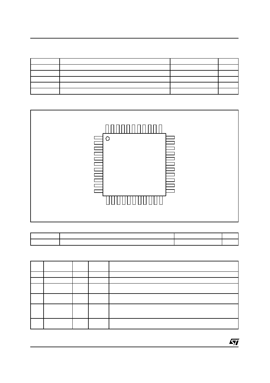
TQFP44
(10 x 10)
TDA7502
IN-CAR REMOTE AMPLIFIER DSP
PRODUCT PREVIEW
1/8
THERMAL DATA
Symbol
Parameter
Value
Unit
R
th j-amb
Thermal Resistance Junction to Ambient
50
�
C/W
SCKR
LRCKR
SDI2
SDI1
SDI0
SDO2
SDO1
SDO0
SCKT
LRCKT
VDD4
GND4
DBOUT
VDD2
VDD6
MISO
VDD1
DBRQN
TESTEN
1
2
3
4
5
6
7
8
9
10
11
12
13
14
15
16
17
18
19
20
21
22
23
24
25
26
27
28
29
30
31
32
33
34
35
36
37
38
39
40
41
42
43
44
INT
SCANEN
GND2
DBCK
RESET
VDD3
GND3
XTO
XTI
GPIO3
GND6
MOSI
SS
SCK
SDA
SCL
GPIO5
GPIO4
GND1
DBIN
PVCC
PGND
CLKOUT
VDD5
GND5
PIN CONNECTION
ABSOLUTE MAXIMUM RATINGS
Symbol
Parameter
Value
Unit
V
DDC
Core DC Supply voltage
4.6
V
V
DDP
Pads DC Supply voltage
4.6
V
V
I
, V
IN
Digital or analog input voltage
-0.5 to (V
DDP
+0.5)
V
T
op
Operative temperature range
-40 to 85
�
C
T
stg
Storage temperature range (plastic)
-55 to 150
�
C
PIN DESCRIPTION
N.
Name
Type
Reset
Status (1)
Function
1
VDD1
I
�
3.3V core supply.
2
GND1
I
�
Core ground.
3
INT
I/O
�
External interrupt line (Input/Output). When this line is asserted low, the
DSP may be interrupted. Acts as IRQA line of DSP core.
4
SCANEN
I
�
SCAN Enable When active with TESTEN also active, controls the
shifting of the internal scan chains.
5
TESTEN
I
�
Test Enable. When active, puts the chip into test mode and muxes the
XTI clock to all flip-flops. When SCANEN is also active, the scan chain
shifting
6
DBRQN
I
�
Debug Port Request Input. Means of entering the Debug mode of
operation.
TDA7502
2/8

N.
Name
Type
Reset
Status
Function
7
DBOUT/GPIO2
I/O
I
The serial data output for the Debug Port. Can also be used as a GPIO.
8
VDD2
I
�
3.3V core supply.
9
GND2
I
�
Core ground.
10
DBCK/GPIO0
I/O
I
Debug Port Bit Clock/Chip Status 1. The serial clock for the Debug Port
is provided when an input. When an output, provides information about
the chip status. Can also be used as GPIO
11
DBIN/GPIO1
I/O
I
Debug Port Serial Input/Chip Status 0. The serial data input for the
Debug Port is provided when an input. When an output, provides
information about the chip status. Can also be used as GPIO.
12
CLKOUT
O
�
Output Clock.
13
PGND
I
�
PLL Clock Ground Input. Ground connection for oscillator circuit.
14
PVCC
I
�
PLL Clock Power Supply. Positive supply for PLL Clock Oscillator.
15
XTO
O
High
Crystal Oscillator Output. Crystal Oscillator output drive.
16
XTI
I
�
Crystal Oscillator Input. External Clock Input or crystal connection.
17
RESET
I/O
I
System Reset. A logic low level applied to RESET input initializes DSPs.
During Debug Mode if this pin is pulled low in while the DBRQN line is
pulled low then the DSP pointed to by the DBSEL pin will be reset.
18
VDD3
I
�
3.3V Supply.
19
GND3
I
�
Ground.
20
SDI0
I
�
SDI0 is a stereo digital audio data input pin channel 0.
21
SDI1
I
�
SDI1 is a stereo digital audio data input pin channel 1.
22
SDI2
I
�
SDI2 is a stereo digital audio data input pin channel 2.
23
SCKR
I/O
�
SAI receive bit clock. Master or slave.
24
LRCKR
I/O
�
Left-Right clock for SAI Receiver. Master or slave.
25
VDD4
I
�
3.3V Supply.
26
GND4
I
�
Ground.
27
SDO0
O
High
SDO0 is a stereo digital audio data output pin channel 0.
28
SDO1
O
High
SDO1 is a stereo digital audio data output pin channel 1.
29
SDO2
O
High
SDO2 is a stereo digital audio data pin channel 2.
30
VDD5
GND
�
3.3V Supply.
31
GND5
I
�
Ground.
32
LRCKT
I/O
�
SAI transmit left/right clock. Master or slave.
33
SCKT
I/O
�
SAI transmit bit clock. Master or slave.
34
SCL
I/O
�
Clock line for I
2
C bus. Schmitt trigger input.
35
SDA
I/O
�
Data line for I
2
C bus. Schmitt trigger input.
36
SCK
I
�
Bit clock for SPI control interface.
37
SS
I
�
Slave select input pin for SPI control interface.
38
MOSI
I/O
I
Serial Data Output for SPI type serial port when in SPI Master Mode and
Serial Data Input when in SPI Slave Mode.
39
MISO
I/O
I
Serial Data Input for SPI style serial port when in SPI Master Mode and
Serial Data Output when in SPI Slave Mode.
40
VDD6
GND
�
3.3V Supply.
41
GND6
I
�
Ground.
42
GPIO3
I/O
�
This pin is dedicated as general I/O.
43
GPIO4
I/O
�
This pin is dedicated as general I/O.
44
GPIO5
I/O
�
This pin is dedicated as general I/O.
PIN DESCRIPTION (continued)
TDA7502
3/8

RECOMMENDED DC OPERATING CONDITIONS
Symbol
Parameter
Test Condition
Min.
Typ.
Max.
Unit
V
DDC
3.3V Power Supply Voltage
3
3.3
3.6
V
T
j
Operating Junction
Temperature
-40
125
�
C
POWER CONSUMPTION
Symbol
Parameter
Value
Unit
I
dd
Maximum current for core power supply @3.3V
250
mA
Note: 50MHz internal DSP clock at Tamb
FUNCTIONAL DESCRIPTION
The TDA7502 contains one DSP Core and asso-
ciated peripherals.
24-BIT DSP CORE.
The DSP core is used to process the converted
analog audio data coming from the CODEC chip
via the SAI and return it for analog conversion.
Functions such as volume, tone, balance, and
fader control, as well as spatial enhancement and
general purpose signal processing may be per-
formed by the DSP.
Some capabilities of the DSPs are listed below:
Single cycle multiply and accumulate with con-
vergent rounding and condition code genera-
tion
2 x 56-bit Accumulators
Double precision multiply
Scaling and saturation arithmetic
48-bit or 2 x 24-bit parallel moves
64 interrupt vector locations
Fast or long interrupts possible
Programmable interrupt priorities and masking
8 each of Address Registers, Address Offset
Registers and Address Modulo Registers
Linear, Reverse Carry, Multiple Buffer Modulo,
Multiple Wrap-around Modulo address arith-
metic
Post-increment or decrement by 1 or by offset,
Index by offset, predecrement address
Repeat instruction and zero overhead DO
loops
Hardware stack capable of nesting combina-
tions of 7 DO loops or 15 interrupts/subrou-
tines
Bit manipulation instructions possible on all
registers and memory locations. Also Jump on
bit test.
4 pin serial debug interface
Debug access to all internal registers, buses
and memory locations
5 word deep program address history FIFO
Hardware and software breakpoints for both
program and data memory accesses
Debug Single stepping, Instruction injection
and Disassembly of program memory
DSP PERIPHERALS
There are a number of peripherals that are tightly
coupled to the DSP Core. Each of the peripherals
are listed below and described in the following
sections.
512 x 24-Bit X-RAM.
512 x 24-Bit Y-RAM.
3072 x 24-Bit Program RAM
128 x 24-Bit Boot ROM.
Serial Audio Interface (SAI)
Single Debug Port
Programmable Control Interface (SPI/I
2
C)
GPIO
DATA AND PROGRAM MEMORY
Each of the memories are described below.
512 x 24-Bit X-RAM (XRAM)
This is a 512 x 24-Bit Single Port SRAM used for
storing coefficients. The 16-Bit XRAM address,
XABx(15:0) is generated by the Address Genera-
tion Unit of the DSP core. The 24-Bit XRAM Data,
XDBx(23:0), may be written to and read from the
Data ALU of the DSP core. The XDBx Bus is also
connected to the Internal Bus Switch so that it
can be routed to and from all peripheral blocks.
512 x 24 Bit Y-RAM (YRAM)
This is a 512 x 24-Bit Single Port SRAM used for
storing
coefficients.
The
16-Bit
address,
YABx(15:0) is generated by the Address Genera-
tion Unit of the DSP core. The 24-Bit Data,
YDBx(23:0), is written to and read from the Data
TDA7502
4/8

ALU of the DSP core. The YDBx Bus is also con-
nected to the Internal Bus Switch so that it can be
routed to and from other blocks.
3072 X 24-Bit Program RAM
This is a 3072 x 24-Bit Single Port SRAM used
for storing and executing program code. The 16-
Bit PRAM Address, PABx(15:0) is generated by
the Program Address Generator of the DSP core
for Instruction Fetching, and by the AGU in the
case of the Move Program Memory (MOVEM) In-
struction. The 24-Bit PRAM Data (Program
Code), PDBx(23:0), can only be written to using
the MOVEM instruction.
During instruction fetching the PDBx Bus is
routed to the Program Decode Controller of the
DSP core for instruction decoding.
Spare space in the Program area may be used
as data memory to implement delay lines for ex-
ample.
128 x 24-Bit Bootstrap ROM (PROM)
This is a 128 x 24-Bit factory programmed Boot
ROM used for storing the program sequence for
initializing the DSP.
Essentially this consists of a routine that is called
when the DSP comes out of reset. There are
three different boot modes supported by the boot
ROM, one boots directly into PRAM, the second
boots over the I
2
C bus and the third boots are the
SPI bus. The boot mode is selected by the levels
on GPIO3 and GPIO5
Serial Audio Interface (SAI)
The SAI is used to deliver digital audio to the
DSPs from an external source. Once processed
by the DSPs, it can be returned through this inter-
face. The features of the SAI are listed below.
Three Synchronized Stereo Data Transmission
Lines
Three Synchronized Stereo Data Reception
Lines
Master/Slave operating modes
Transmit and Receive Interrupt Logic triggers
on Left/Right data pairs
Receive and Transmit Data Registers have
two locations to hold left and right data.
Serial Peripheral Interface
The DSP core requires a serial interface to re-
ceive commands and data over the LAN. During
an SPI transfer, data is transmitted and received
simultaneously. A serial clock line synchronizes
shifting and sampling of the information on the
two serial data lines. A slave select line allows in-
dividual selection of a slave SPI device.
When an SPI transfer occurs an 8-bit word is
shifted out one data pin while another 8-bit char-
acter is simultaneously shifted in a second data
pin.
The central element in the SPI system is the shift
register and the read data buffer. The system is
single buffered in the transfer direction and dou-
ble buffered in the receive direction.
I
2
C Interface
The inter Integrated Circuit bus is a single bidirec-
tional two-wire bus used for efficient inter IC con-
trol. All I
2
C bus compatible devices incorporate
an on-chip interface which allows them communi-
cate directly with each other via the I
2
C bus.
Every component hooked up to the I
2
C bus has
its own unique address whether it is a CPU,
memory or some other complex function chip.
Each of these chips can act as a receiver and /or
transmitter on its functionality.
General Purpose Input/Output
The DSP requires a set of external general pur-
pose input/output lines, and a reset line. These
signals are used by external devices to signal
events to the DSP. The GPIO lines are imple-
mented as DSP 's peripherals
PLL Clock Oscillator
The PLL Clock Oscillator can accept an external
clock at XTI or it can be configured to run an in-
ternal oscillator when a crystal is connected
across pins XTI & XTO. There is an input divide
block IDF (1 -> 32) at the XTI clock input and a
multiply block MF (33 -> 128) in the PLL loop.
Hence the PLL can multiply the external input
clock by a ratio MF/IDF to generate the internal
clock. This allows the internal clock to be within 1
MHz of any desired frequency even when XTI is
much greater than 1 MHz. It is recommended that
the input clock is not divided down to less than 1
MHz as this reduces the Phase Detector's update
rate.
The clocks to the DSP can be selected to be
either the VCO output divided by 2 or 4 respec-
tively, or be driven by the XTI pin directly.
The crystal oscillator and the PLL will be gated off
when entering the power-down mode (by setting
bit 1 of the PCON Register).
TDA7502
5/8