 | –≠–ª–µ–∫—Ç—Ä–æ–Ω–Ω—ã–π –∫–æ–º–ø–æ–Ω–µ–Ω—Ç: TDA7522 | –°–∫–∞—á–∞—Ç—å:  PDF PDF  ZIP ZIP |

1/23
PRODUCT PREVIEW
This is preliminary information on a new product now in development. Details are subject to change without notice.
TDA7522
Digital Servo & Decoder
s
BUILT IN 8Bit MICROCONTROLLER
(STANDARD ST7) with:
≠ 24 KByte ROM available for ST7 & Servo-Audio
DSP
≠ 1024Byte RAM, including 128byte stack
≠ 4KByte RAM for CD-Text memory (for 1block)
≠ Built in R-W subcode buffer (Max. 144Byte
8packs) for CD-Text
≠ 24 bit general I/O port (PoartA[7-0], PortB[7-0],
PortC[7-0])
≠ One External Interrupt (16 IRQ encoder inside)
≠ 16bit free running counter timer
≠ 8bit 1ch general purpose A/D
≠ I
2
C bus I/F
≠ Watch dog
≠ Kenwood I/F
s
STAND-BY MODE (Stop all clocks and Shut down power of Peripheral (PON pin))
s
BUILT IN SERVO & AUDIO DIGITAL SIGNAL PROCESSOr (SAC-DSP) inclusive of:
≠ 1024x19bit Program RAM
≠ 512x16bit Coefficient RAM
≠ 1024x20bit Data RAM
≠ 128x6bit Decimation RAM
≠ MAC: 16 bit (Coefficients) x 20 bit (data) multiplier with 38 bit adder
≠ Instruction execution rate as high as 56MIPS
s
BUILT IN PROGRAMMABLE CLOCK GENERATOR PLL
s
PERIPHERALS for CD PLAYER APPLICATION
≠ Data Acquisition, Erasure correction, CLV&CAV controller
≠ Subcode decoder (CD-Text, CD-Graphic I/F)
≠ Shock proof memory controller, Disturbance detector
≠ Decimation filter
s
ACTUATORS DRIVING MODE SELECTABLE between PWM or PDM MODE
s
256Fs / 384Fs (16.9344MHz) CLOCK INPUT.
May 1998
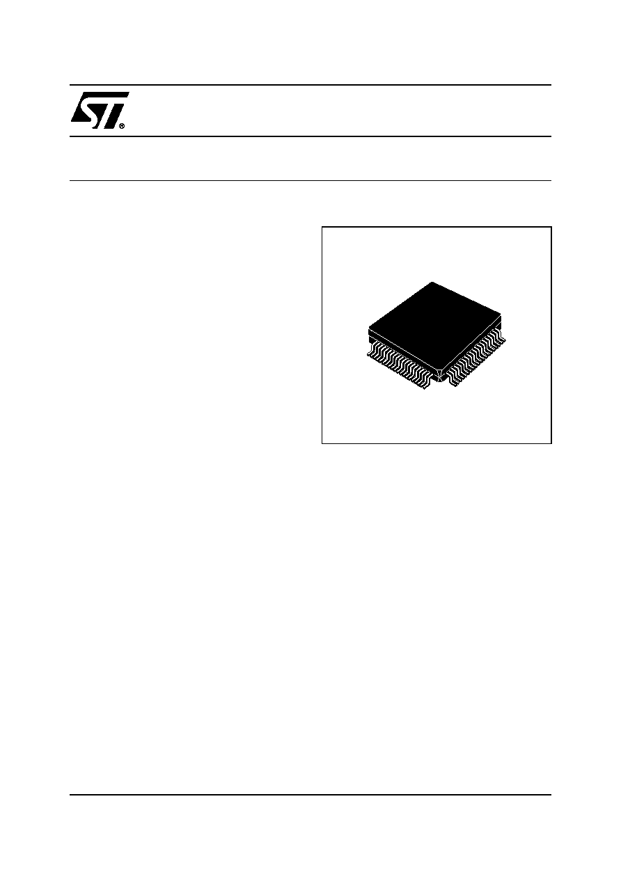
TQFP80
(14 x 14 x 1.40mm body)

TDA7522
2/23
1.0 DESCRIPTION
TDA7522 is a single chip processor consisting of Decoder, Servo and 1bit D/A for 4times CD-ROM / CD-
Audio. Main concept of this IC is that it is based on embedded System Micro Controller which allows cus-
tomer to develop system software very easily: just based on provided commands. Further the microcon-
troller is fully customer dedicated in terms of both software and general purpose Port.
By combination of ST Analog front-end IC (TDA7521), all CD functions including Shock Proof Memory
Controller and CD-Text function can be realized.
The TDA7522 portfolio is constituted by three different versions:
≠ 'development': which gives the possibility to have at disposal the complete sw development environ-
ment, by means of a dedicated package
≠ `in field development': standard package but with selection of program memory: on chip RAM, on chip
ROM. The program RAM is fully patchable through the standard IIC interface, giving the possibility of
sw changing while chip is working in the real environment.
≠ `production': standard package, but with software permanently stored in the on chip ROM.
2.0 TECHNOLOGY
All version are produced using the HCMOS6 0.35um technology which works @3.3Vdc; to avoid interface
problem with existing logics, all digital Inputs are 5V tolerant. When interfacing logic on TDA7522 outputs,
user should take care of output levels that are at CMOS level @3.3V. Depending on output type the I
ol
and I
oh
value are guaranteed at 4mA or 8mA; the TDA7522 output driving specification will be included in
a next issue of this data sheet.
3.0 ADDITIONAL FEATURES
s
16Mbit DRAM I/F allows maximum 9 seconds shock proof
s
Built-in 1bit Delta Sigma modulation for DAC
s
Subcode P,Q and R-W decoding
s
Error Correction is capable of Dual C1 and quadruple C2 erasure corrections
s
Jitter absorbing capability: +/- 6 frames
s
Automatic fine gain/balance/offset adjustment for tracking and focus servos
s
Built-in Digital Silence detection
s
Built-in EFM Demodulation/Sync Rear and Forward protection
s
Soft audio mute
s
Built-in Digital PLL with large capture range from 0.5 to 4 times speed
s
Digital Servo control for all servo loops
s
Capable of 2x and 4x speeds for shock proof and CD-ROM applications
s
Capable of wide temperature range (-40C to +85C) stable operation
s
Fast access times for CD-ROM applications due to wide Capture range and CAV mode run at max 4
times overspeed
s
CLV or CAV (lock-to-disk mode) spindle servo operations
s
Digital Output SPDIF (DIT CP340)
s
Sony LSI Output Interface (for Audio & CD-ROM)
s
Pulsate SLED mode support
s
Built in 8times Audio Over sampling filter.

3/23
TDA7522
Figure 1. Pin Connection
PIN
_
KD
MPH
Y
S
21
PIN
_
P
O
N
2
2
P
I
N_A
V
DD
_1
2
3
PI
N
_
XT
I
2
4
PIN
_
XT
O
PI
N
_
A
V
S
S
_
1
26
P
I
N
_
KAD
C
_
VR
H
2
7
PI
N
_
KAD
C
_
VR
L
2
8
PI
N
_
KAD
C
_
IN
2
9
P
I
N_
NRE
S
E
T
30
TDA7522
80-pin
PI
N
_
T
EST
EN
31
P
I
N_
CO
RE
_V
D
D
_
2
32
PIN
_
C
O
R
E
_
VSS_
2
33
PIN
_
SC
K
3
4
PIN
_
S
D
A
3
5
PIN
_
S
C
AN
EN
3
6
PIN
_
KA
SEL
3
7
PIN
_
KT
E
S
T
3
8
PIN
_
K
SEAR
C
H
3
9
PI
N
_
MST
O
P
4
0
P
I
N_
DR
D3
80
P
I
N_
DR
D2
79
P
I
N_
DR
D1
78
P
I
N_
DR
D0
77
P
I
N_
DR
A
0
76
P
I
N_
DR
A
1
75
P
I
N_
DR
A
2
74
P
I
N_
DR
A
3
73
P
I
N_
DR
A
4
72
P
I
N_
CO
RE
_V
S
S
_4
71
P
I
N_
CO
RE
_V
D
D
_
4
70
P
I
N_
DR
A
5
69
P
I
N_
DR
A
6
68
P
I
N_
DR
A
7
67
P
I
N_
DR
A
8
66
P
I
N_
DR
A
9
65
PIN_DRA10
64
PIN_DRA11
63
PIN_RAS
62
PIN_CAS
61
PIN_MUTER
20
PIN_MUTEL
19
PIN_C2P0
18
PIN_LRCK
17
PIN_BSL_SAK48
16
PIN_BSR_SDK48
15
PIN_CLKOUT
14
PIN_DGTSYNC
13
PIN_DGTLIN7
12
PIN_CORE_VSS_1
11
PIN_CORE_VDD_1
10
PIN_DGTLIN_6
9
PIN_DGTLIN5
8
PIN_DGTLIN4
7
PIN_DGTLIN3
6
PIN_DGTLIN2
5
PIN_DGTLIN1_UF
4
PIN_DGTLIN0_OF
3
PIN_SERCK
2
PIN_SERDA
1
PIN
_
SPD
L
41
PIN
_
T
F
S
R
42
PIN
_
F
F
S
R
43
P
I
N
_
SF
SR
44
PIN_SLEDL
45
PIN_K_VER_HOR
46
PIN_WFCK
47
PIN_EXCK
48
PIN_SBSO
49
PIN_CORE_VDD_3
50
PIN_CORE_VSS_3
51
PIN_SCOR
52
PIN_DOUT
53
PIN_CS
54
PIN_SRQ
55
PIN_DATAS
56
PIN_DATAM
57
PIN_CLK
58
PIN_DRS
59
PIN_DWR
60
25
TDA7522 general overview is reported below.
REMARK: CONSIDERING THE SELECTION DONE BY CUSTOMER, THE DRAM I/F COULD BE
SLIGTHY MODFIED. DETAILS WILL BE GIVEN IN A LATER ISSUE OF DATA SHEET.

TDA7522
4/23
Table 1. Pin Description
Pin Number
Name
Function
Description
01
SERDA
I/O
Data line for Serial I/F
02
SERCK
O
Clock line for Serial I/F
03
DGTLIN0_OF
I
HF bit 0 and Servo overflow
04
DGTLIN1_UF
I
HF bit 1 and Servo underflow
05
DGTLIN2
I
HF bit 2 and Servo bit 0
06
DGTLIN3
I
HF bit 3 and Servo bit 1
07
DGTLIN4
I
HF bit 4 and Servo bit 2
08
DGTLIN5
I
HF bit 5 and Servo bit 3
09
DGTLIN6
I
HF bit 6 and Servo bit 4
10
CORE_VDD_1
Vdd
Digital Power supply
11
CORE_VSS_1
Gnd
Digital Ground
12
DGTLIN7
I
HF bit 7 and Servo bit 5
13
DGTSYNC
I
Sync strobe for Multiplexer
14
CLKOUT
O
System clock output to TDA7521
15
BSR_SDK48
O
LSI I/F clock output or
DAC bit stream right channel output
16
BSL_SAK48
O
LSI I/F data output or DAC bit stream left channel output
17
LRCK
O
LSI I/F L/R signal
18
C2PO
O
Validity flag output for CD-ROM decoder
19
MUTEL
O
Mute left signal (active high)
20
MUTER
O
Mute right signal (Active high)
21
KDMPHYS
I/O
De-emphasis indication or ST7 GPIO PA2
22
PON
I/O
System shutdown pin for power saving mode or
ST7 GPIO PC7
23
AVDD_1
Vdd
Analog power supply
24
XTI
I
Crystal input
25
AVSS_1
Gnd
Analog ground
26
XTO
O
Crystal output
27
KADC_VRH
I
ADC top reference Voltage input
28
KADC_VRL
I
ADC bottom reference Voltage input
29
KADC_IN
I
ADC input
30
CORE_VDD_2
Vdd
Digital Power supply
31
CORE_VSS_2
Gnd
Digital Ground
32
Nreset
I
Hardware reset

5/23
TDA7522
33
TESTEN
I
Test enable signal (Active low)
34
SCK
I
IIC I/F clock signal
35
SDA
I/O
IIC I/F data
36
SCANEN
I
Scan enable (active high) or select DRAM outputs as TEST
outputs when TESTEN is inactive
37
KASEL
I/O
DAC polarity selection pin or ST7 GPIO PA0
38
KTEST
I/O
User test mode selection or ST7 GPIO PA1
39
KSEARCH
I/O
Gain change during search or ST7 GPIO PA3
40
MSTOP
I/O
interrupt request/stand-by pin or ST7 GPIO PC5
41
SLEDL
I/O
SLED limit switch or ST7 GPIO PC6
42
K_VER_HOR
I/O
Indication of vertical or horizontal operation
or ST7 GPIO PA4
43
WFCK
O
Write Frame clock for Subcode P-W output
44
EXCK
I
SBSO readout clock input
45
SBSO
O
Subcode P-W serial output
46
SCOR
O
Subcode sync output
47
DOUT
O
SPDIF Digital audio output
48
CS
I/O
ST7 GPIO PC4
49
SRQ
I/O
ST7 GPIO PC3
50
CORE_VDD_3
Vdd
Digital Power supply
51
CORE_VSS_3
Gnd
Digital Ground
52
DATAS
I/O
ST7 GPIO PC2
53
DATAM
I/O
ST7 GPIO PC1
54
CLK
I/O
ST7 GPIO PC0
55
DRS
I/O
Shock proof memory Read control
56
DWR
I/O
Shock proof memory Write control
57
CAS
I/O
Shock proof memory Column address select
58
RAS
I/O
Shock proof memory Row address select
59
DRA11
I/O
DRAM Address 11
60
DRA10
I/O
DRAM Address 10
61
DRA9
I/O
DRAM Address 9 or Mirror signal output
62
DRA8
I/O
DRAM Address 8 or TZC (Tracking Zero Cross) signal output
63
DRA7
I/O
DRAM Address 7 or FOK (Focus OK) signal output
64
DRA6
I/O
DRAM Address 6 or ST7 GPIO PB7 or PLLINF signal output
Pin Number
Name
Function
Description


