 | ÐлекÑÑоннÑй компоненÑ: TDA7575PD | СкаÑаÑÑ:  PDF PDF  ZIP ZIP |
Äîêóìåíòàöèÿ è îïèñàíèÿ www.docs.chipfind.ru
1/17
TDA7575PD
March 2004
DMOS POWER OUTPUT
NON-SWITCHING HI-EFFICIENCY
SINGLE-CHANNEL 1
DRIVING CAPABILITY
HIGH OUTPUT POWER CAPABILITY 2x28W/
4
@ 14.4V, 1KHZ, 10% THD, 2x40W/4 EIAJ
MAX. OUTPUT POWER 2x75W/2
, 1x150W/1
SINGLE-CHANNEL 1
DRIVING CAPABILITY
84W UNDISTORTED POWER
FULL I
2
C BUS DRIVING WITH 4 ADDRESS
POSSIBILITIES:
ST-BY, PLAY/MUTE, GAIN 12/26dB, FULL
DIGITAL DIAGNOSTIC
POSSIBILITY TO DISABLE THE I2C
DIFFERENTAL INPUTS
FULL FAULT PROTECTION
DC OFFSET DETECTION
TWO INDEPENDENT SHORT CIRCUIT
PROTECTIONS
CLIPPING DETECTOR PIN WITH
SELECTABLE THRESHOLD (2%/10%)
ST-BY/MUTE PINS
DESCRIPTION
The TDA7575PD is a new BCD technology DUAL
BRIDGE type of car radio amplifier in PowerSO36
package specially intended for car radio applications.
Thanks to the DMOS output stage the TDA7575PD
has a very low distortion allowing a clear powerful
sound. Among the features, its superior efficiency
performance coming from the internal exclusive
structure, makes it the most suitable device to simpli-
fy the thermal management in high power sets.The
dissipated output power under average listening con-
dition is in fact reduced up to 50% when compared to
the level provided by conventional class AB solu-
tions.
This device is equipped with a full diagnostic array
that communicates the status of each speaker
through the I
2
C bus. The TDA7575PD has also the
possibility of driving loads down to 1
paralleling the
outputs into a single channel. It is also possible to dis-
able the I
2
C and control the TDA7575PD by means of
the usual ST-BY and MUTE pins.
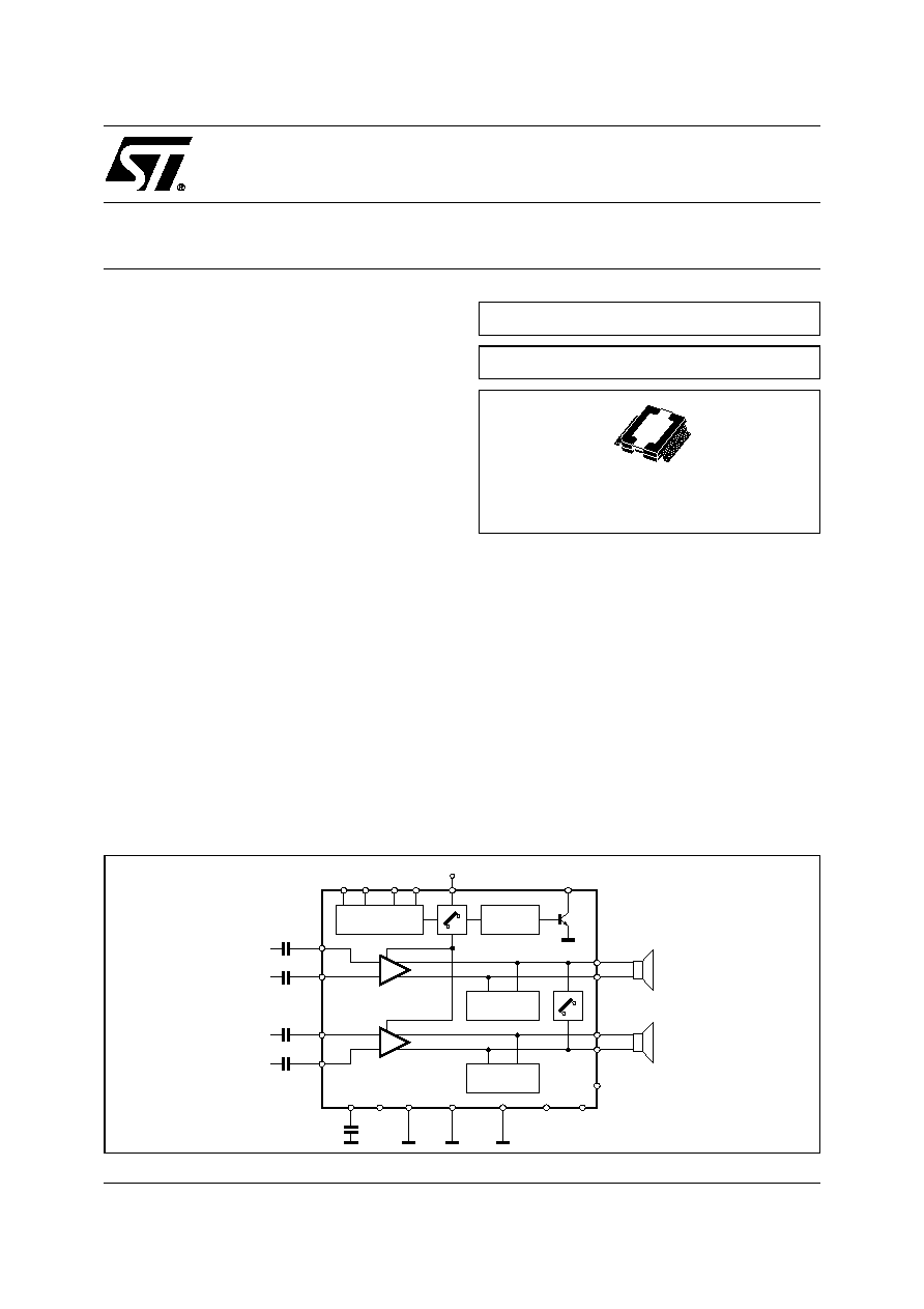
MULTIPOWER BCD TECHNOLOGY
MULTIFUNCTION DUAL BRIDGE POWER AMPLIFIER
WITH INTEGRATED DIGITAL DIAGNOSTICS
BLOCK DIAGRAM
I
2
CBUS
A
B
CLK
ADDRESS
DATA
VCC
CD_OUT
V
S
OUT1+
OUT1-
OUT2+
OUT2-
CLIP
DETECTOR
SHORT CIRCUIT
PROTECTION
SHORT CIRCUIT
PROTECTION
IN1+
SVR
S_GND
I
2
C EN
PW_GND
TAB
ST-BY/HE
1
MUTE
IN1-
IN2+
IN2-
D01AU1269
MOSFET OUTPUT POWER STAGE
PowerSO36 (Slug up)
ORDERING NUMBER: TDA7575PD
TDA7575PD
2/17
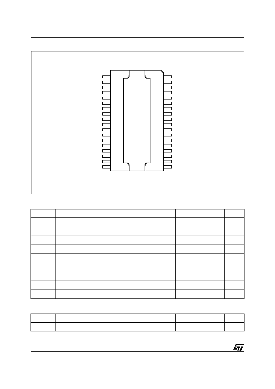
PIN CONNECTION (Top view)
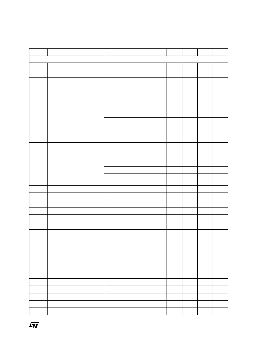
ABSOLUTE MAXIMUM RATINGS
THERMAL DATA
Symbol
Parameter
Value
Unit
V
op
Operating Supply Voltage
18
V
V
S
DC Supply Voltage
28
V
V
peak
Peak Supply Voltage (for t = 50ms)
50
V
V
CK
CK pin Voltage
6
V
V
DATA
Data Pin Voltage
6
V
I
O
Output Peak Current (not repetitive t = 100ms)
8
A
I
O
Output Peak Current (repetitive f > 10Hz)
6
A
P
tot
Power Dissipation T
case
= 70°C
86
W
T
stg
, T
j
Storage and Junction Temperature
-55 to 150
°C
Symbol
Parameter
Value
Unit
Rth j-case
Thermal Resistance Junction-case
Max
1
°C/W
TAB
18
16
17
15
6
5
4
3
2
21
22
31
32
33
35
34
36
20
1
19
OUT2+
D01AU1270
9
8
7
28
29
30
10
27
14
12
11
23
25
26
13
24
IN2+
IN2-
I2C-EN
CD-OUT
1-OHM
ST_BY
MUTE
IN1-
IN1+
SVR
N.C.
N.C.
N.C.
N.C.
SGND
CK
DATA
OUT1+
OUT1+
VCC
PWGND
A
PWGND
VCC
VCC
OUT2+
OUT1-
OUT2-
OUT2-
OUT1-
VCC
PWGND
PWGND
B
3/17
TDA7575PD
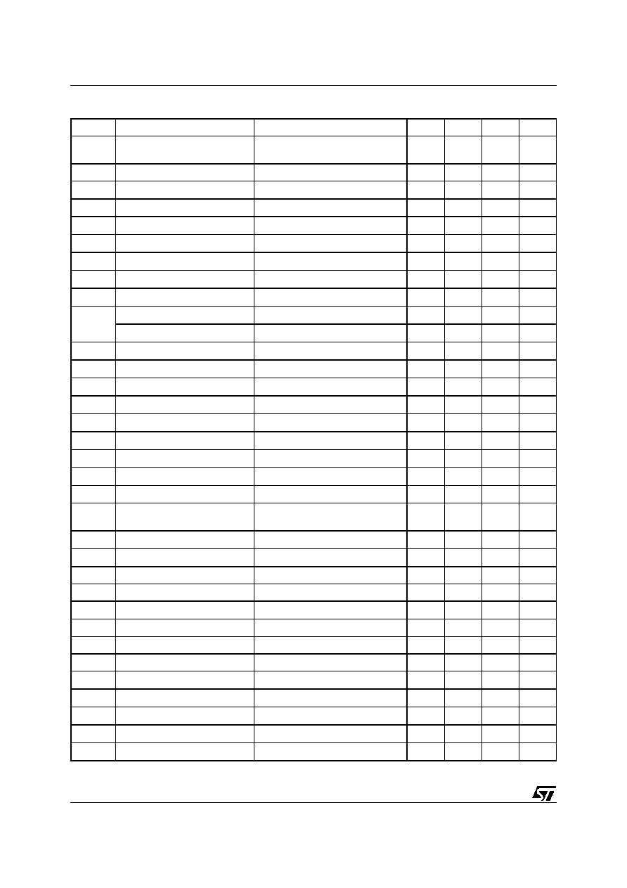
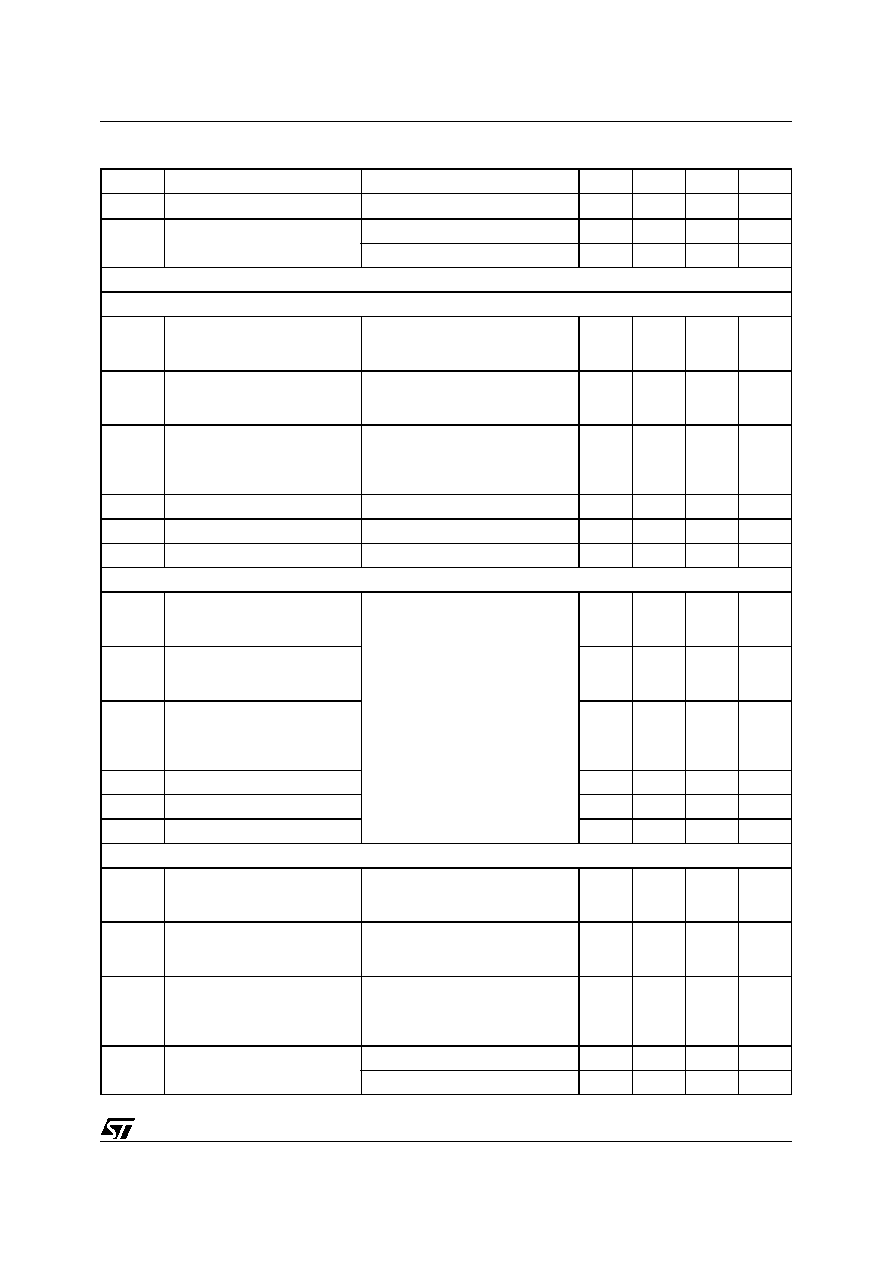
Symbol
Parameter
Test Condition
Min.
Typ.
Max.
Unit
POWER AMPLIFIER
V
S
Supply Voltage Range
8
18
V
I
d
Total Quiescent Drain Current
50
130
200
mA
Po
Output Power
EIAJ (V
S
= 13.7V)
35
40
W
THD = 10%
THD = 1%; BTL MODE
25
28
22
W
W
R
L
= 2
; EIAJ (V
S
= 13.7V)
R
L
= 2
; THD 10%
R
L
= 2
; THD 1%
R
L
= 2
; MAX POWER
60
45
70
65
50
37
75
W
W
W
W
Single channel configuration
(1
pin >2.5V); R
L
= 1
;
EIAJ (V
S
= 13.7V)
THD 3%
MAX POWER
125
80
140
130
84
150
W
W
W
THD
Total Harmonic Distortion
P
O
= 1-12W; STD MODE
HE MODE; P
O
= 1-2W
HE MODE; P
O
= 4-8W
0.03
0.03
0.5
0.1
0.1
%
%
%
P
O
= 1-12W, f = 10kHz
0.15
0.5
%
R
L
= 2; HE MODE; Po = 3W
0.03
0.5
%
Single channel configuration
(1
pin >2.5V); R
L
= 1; P
O
= 4-30W
0.02
0.1
%
C
T
Cross Talk
R
g
= 600
; P
O
= 1W
60
75
dB
R
IN
Input Impedance
60
100
130
K
G
V1
Voltage Gain 1 (default)
25
26
27
dB
G
V1
Voltage Gain Match 1
-1
0
1
dB
G
V2
Voltage Gain 2
11
12
13
dB
G
V2
Voltage Gain Match 2
-1
0
1
dB
E
IN1
Output Noise Voltage Gain 1
Rg = 600
; Gv = 26dB
filter 20 to 22kHz
40
60
µV
E
IN2
Output Noise Voltage Gain 2
Rg = 600
; Gv = 12dB
filter 20 to 22kHz
15
25
µV
SVR
Supply Voltage Rejection
f = 100Hz to 10kHz; V
r
= 1Vpk;
R
g
= 600
50
60
dB
BW
Power Bandwidth
(-3dB)
100
KHz
A
SB
Stand-by Attenuation
90
100
dB
I
SB
Stand-by Current Consumption
2
20
µA
A
M
Mute Attenuation
80
90
dB
V
OS
Offset Voltage
Mute & Play
-45
0
45
mV
V
AM
Min. Supply Mute Threshold
7
7.5
8
V
CMRR
Input CMRR
V
CM
= 1Vpk-pk; Rg = 0
50
60
dB
ELECTRICAL CHARACTERISTCS: (V
S
=14.4V; f=1KHz; R
L
=4
; Tamb= 25°C unless otherwise specified)
TDA7575PD
4/17
V
MC
Maximum common mode input
level
f = 1kHz
1
Vrms
SR
Slew Rate
1.5
4
V/
µs
V
PM
Mute/Unmute Transient
A-weighted
-100
0
100
mVpp
V
TO
Mute/Stand-by Transient
A-weighted
-100
0
100
mVpp
T
ON
Turn on Delay
D2 (IB1) 0 to 1
15
40
ms
T
OFF
Turn off Delay
D2 (IB1) 1 to 0
15
40
ms
V
OFF
St-By pin for St-By
0
1.5
V
V
SB
St-By pin for standard bridge
3.5
5
V
V
HE
St-By pin for Hi-eff
7
18
V
I
O
St-By pin Current
1.5 < V
stby/HE
< 18V
7
160
200
µA
St-By Pin Current
V
stby
< 1.5V
-10
0
10
µA
V
m
Mute pin voltage for mute mode
0
1.5
V
V
m
Mute pin voltage for play mode
3.5
18
V
I
m
Mute pin current (ST_BY)
V
mute
= 0V, V
stby
< 1.5V
-5
0
5
µA
I
m
Mute pin current (operative)
0V < V
mute
< 18V, V
stby
> 3.5V
65
100
µA
V
I2C
I2C pin voltage for I2C disabled
0
1.5
V
V
I2C
I2C pin voltage for I2C enabled
2.5
18
V
I2C
I2C pin current (stby)
0V < I2C EN < 18V, V
stby
< 1.5V
-5
0
5
µA
I2C
I2C pin current (operative)
I2C EN <18V, V
stby
>3.5V
7
11
15
µA
V
1OHM
1OHM pin voltage for 2ch mode
0
1.5
V
V
1OHM
1OHM pin voltage for 1ohm
mode
2.5
18
V
I
1OHM
1OHM pin current (stby)
0V < 1OHM <18V, V
stby
< 1.5V
-5
0
5
µA
I
1OHM
1OHM pin current (operative)
1OHM <18V, V
stby
> 3.5V
7
11
15
µA
La
A Pin Voltage
Low logic level
0
1.5
V
Ha
High logic level
2.5
18
V
Ia
A Pin Current (ST-BY)
0V < A < 18V, V
stby
< 1.5V
-5
0
5
µA
Ia
A Pin Current (Operative)
A<18V, V
stby
> 3.5V
7
11
15
µA
Lb
B Pin Voltage
Low logic level
0
1.5
V
Hb
High logic level
2.5
18
V
Ib
B Pin Current (ST-BY)
0V < B < 18V, V
stby
< 1.5V
-5
0
5
µA
Ib
B Pin Current (Operative)
B < 18V, V
stby
> 3.5V
7
11
15
µA
T
W
Thermal warning
150
°C
T
PI
Thermal Protection intervention
170
°C
I
CDH
Clip Pin High Leakage Current
CD off, 0V < V
CD
< 5.5V
-15
0
15
µA
Symbol
Parameter
Test Condition
Min.
Typ.
Max.
Unit
ELECTRICAL CHARACTERISTCS: (continued)
5/17
TDA7575PD
I
CDL
Clip Pin Low Sink Current
CD on; V
CD
< 300mV
1
mA
CD
Clip detect THD level
D0 (IB1) = 0
0.8
1.3
2.5
%
D0 (IB1) = 1
5
10
15
%
(*) ST-BY Pin high enables I2C bus; ST-BY Pin low puts the device in ST-BY condition.(see "prog" for more details)
TURN ON DIAGNOSTICS (Power Amplifier Mode)
Pgnd
Short to GND det. (below this
limit, the Output is considered in
Short Circuit to GND)
Power Amplifier in st-by condition
1.2
V
Pvs
Short to Vs det. (above this
limit, the Output is considered in
Short Circuit to VS)
V
s
-0.9
V
Pnop
Normal operation
thresholds.(Within these limits,
the Output is considered
without faults).
1.8
V
s
-1.5
V
Lsc
Shorted Load det.
0.5
Lop
Open Load det.
130
Lnop
Normal Load det.
1.5
70
TURN ON DIAGNOSTICS (Line Driver Mode)
Pgnd
Short to GND det. (below this
limit, the Output is considered in
Short Circuit to GND)
Power Amplifier in st-by
1.2
V
Pvs
Short to Vs det. (above this
limit, the Output is considered in
Short Circuit to VS)
V
s
-0.9
V
Pnop
Normal operation
thresholds.(Within these limits,
the Output is considered
without faults).
1.8
V
s
-1.5
V
Lsc
Shorted Load det.
1.5
Lop
Open Load det.
400
Lnop
Normal Load det.
4.5
200
PERMANENT DIAGNOSTICS (Power Amplifier Mode or Line Driver Mode)
Pgnd
Short to GND det. (below this
limit, the Output is considered in
Short Circuit to GND)
Power Amplifier in Mute or Play
condition, one or more short circuits
protection activated
1.2
V
Pvs
Short to Vs det. (above this
limit, the Output is considered in
Short Circuit to VS)
V
s
- 0.9
V
Pnop
Normal operation
thresholds.(Within these limits,
the Output is considered
without faults).
1.8
V
s
-1.5
V
Lsc
Shorted Load det.
Pow. Amp. mode
0.5
Line Driver mode
1.5
Symbol
Parameter
Test Condition
Min.
Typ.
Max.
Unit
ELECTRICAL CHARACTERISTCS: (continued)