 | –≠–ª–µ–∫—Ç—Ä–æ–Ω–Ω—ã–π –∫–æ–º–ø–æ–Ω–µ–Ω—Ç: TDA8196 | –°–∫–∞—á–∞—Ç—å:  PDF PDF  ZIP ZIP |
TDA8196
AUDIO SWITCH AND DC VOLUME CONTROL FOR TV
May 1996
30k
15k
IMPEDANCE
ADAPTER
S WITCH
15k
IMPEDANCE
ADAPTER
REFERENCE
VOLTAGE
AUDIO
OUT
47
µ
F
AUDIO
INPUT (2)
AUDIO
INPUT (1)
S WITCHING CONTROL ( V
S W
)
6.6V
V
S
3
4
2
7
5
6
8
1
V
C
8196-02.EPS
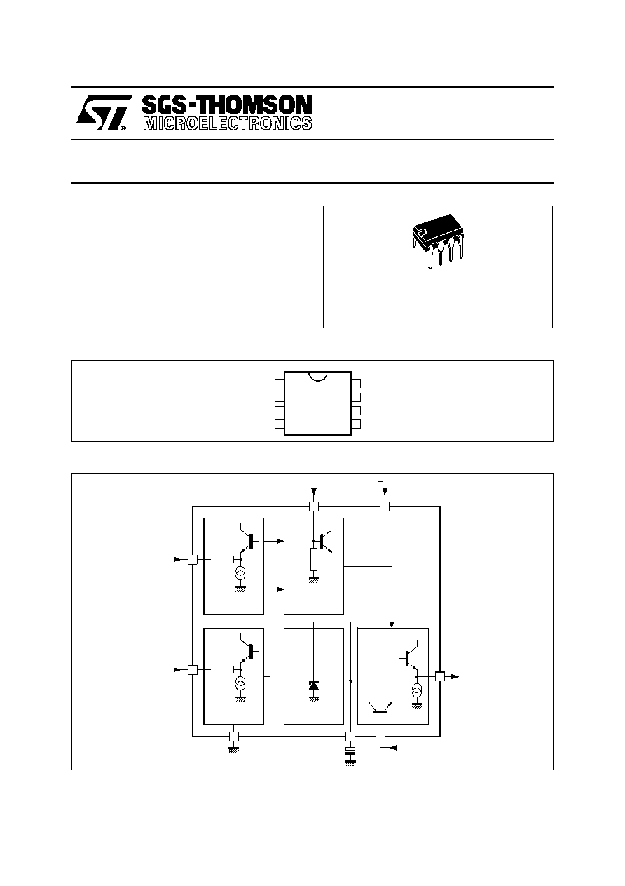
BLOCK DIAGRAM
1
2
3
4
8
7
6
5
AUDIO OUT
GND
VOLUME CONTROL
AUDIO INPUT (2)
SWITCHING CO NTROL
AUDIO INPUT (1)
S
+V
C
REF
8196-01.EPS
PIN CONNECTION (top view)
.
TWO AUDIO INPUTS WITH SWITCHING
FACILITIES FULLY COMPATIBLE WITH THE
SCART EUROPEAN NORM EN 50049
.
DC VOLUME CONTROL
DIP8
(Plastic Package)
ORDER CODE : TDA8196
DESCRIPTION
The TDA8196 is a monolithic integrated circuit in
DIP8 package intended for TV applications.
1/5
ABSOLUTE MAXIMUM RATINGS
Symbol
Parameter
Value
Unit
V
s
Supply Voltage (pin 1)
16
V
T
stg
, T
j
Storage and Junction Temperature
≠ 55 to 125
∞
C
T
amb
Operating Ambient Temperature
0 to 70
∞
C
8196-01.TBL
THERMAL DATA
Symbol
Parameter
Value
Unit
R
thj-amb
Thermal Resistance Junction-ambient
Max
200
∞
C/W
8196-02.TBL
ELECTRICAL CHARACTERISTICS
(refer to the test circuit, V
S
= 12V, T
amb
= 25
o
C unless otherwise specified)
Symbol
Parameter
Pin
Test Conditions
Min.
Typ.
Max.
Unit
V
S
Supply Voltage
1
10.8
12
13.2
V
I
S
Supply Current
1
V
i
= 0, V
C
= 0.5V
12
mA
V
R
Reference Voltage
5
6.6
V
V
SW
Switching Voltage
Audio Input 1
Audio Input 2
3
0
8
5
12
V
V
R
SW
Switching Input Resistance
3
V
SW
= 12V
20
30
k
C
SW
Switching Input Capacitance
3
10
pF
C
t
Crosstalk between Switched
Inputs
Selective Volmeter
(B
W
= 8Hz), see Fig.1
70
90
dB
V
i
Audio Input Amplitude (1 or 2)
4
2
0.5
2
V
RMS
R
i
Audio Input Resistance (1 or 2)
4
2
10
13
k
K
min
Output / Input Gain for Max Vol
0
dB
R
O
Audio Output Resistance
8
0.2
1
k
K
V
Attenuation Range
Selective Volmeter
(B
W
= 8Hz), see Fig.2
70
90
dB
V
C
Control Voltage Range
K
V
= K
MAX
(Vol. min)
K
V
= K
MIN
(Vol. max)
6
0.5
4.5
V
V
THD
Distortion
8
V
i
= 2 V
RMS
@ V
C
= 4.5V
0.4
1
%
En
Output Noise Level
8
DIN45405
V
C
= 0.5V Weighted
40
µ
V
RMS
En
Output Noise Level
8
DIN45405
V
C
= 4.5V Weighted
120
µ
V
RMS
K
V
T
a
Vol. Attenuation Thermal Drift
T
amb
= 0 to 70
o
C
K
V
= 30dB, see Fig.3
0.04
dB/
o
C
SVR
Supply Voltage Rejection
8
V
C
= 0.5V, f = 100Hz
V
ripple
= 1V
PP
Selective Volmeter
(B
W
= 8Hz), see Fig.4 and 5
38
dB
V
O
Output DC Shift
8
V
C
= 0.5 + 4.5V, V
i
= 2 V
RMS
0.25
V
8196-03.TBL
TDA8196
2/5
R
L
10k
4
2
SWITCH
VOLUME
CONTROL
8
3
5
6
1
7
VOLUME
CONTROL
(0.5 to 4.5)
OUTP UT
C4
100
µ
F
C3 10
µ
F
C5 1
µ
F
C1 2.2
µ
F
C2 2.2
µ
F
R1
1k
R2
1k
INPUT 1
INPUT 2
V
S
TDA8196
S WITCH
CONTROL
R3
8196-03.EPS
TEST CIRCUIT
-110
-100
-90
-80
-70
-60
10
100
1000
10000
100000
Ct (dB)
F(Hz)
Input 1
Input 2
8196-04.EPS
Figure 1 : TDA8196 Crosstalk
BW = 8Hz
FLAT BAND
V
(V)
C
kV (dB)
-100
-80
-60
-40
-20
0
0
1
2
3
4
5
8196-05.EPS
Figure 2 :
Output Attenuation versus DC Volume
Control Voltage
-1
0
1
0
10
20
30
40
50
60
70
kV(dB)
T
( C)
amb
8196-06.EPS
Figure 3 : K
v
Drift vs. T
amb
Variation
10
20
30
40
50
60
0
100
10
1000
10000
100000
SVR (dB)
Fripple (Hz)
8196-07.EPS
Figure 4 : SVR vs. Ripple Frequency
TDA8196
3/5
SVR 15625Hz
SVR 50Hz
70
60
50
40
30
20
10
0
20
40
60
80
100
SVR (dB)
8196-08.EPS
Figure 5 : SVR vs. Volume Attenuation
4
2
SWITCH
VOLUME
CONTROL
8
3
5
6
1
7
VOLUME
CONTROL
(0.5 to 4.5)
OUTP UT
C5 1
µ
F
C1 2.2
µ
F
C2 2.2
µ
F
INPUT 1
INPUT 2
V
S
C3 47
µ
F
C4
47
µ
F
S WITCH
CONTROL
TDA8196
8196-09.EPS
APPLICATION CIRCUIT
TDA8196
4/5
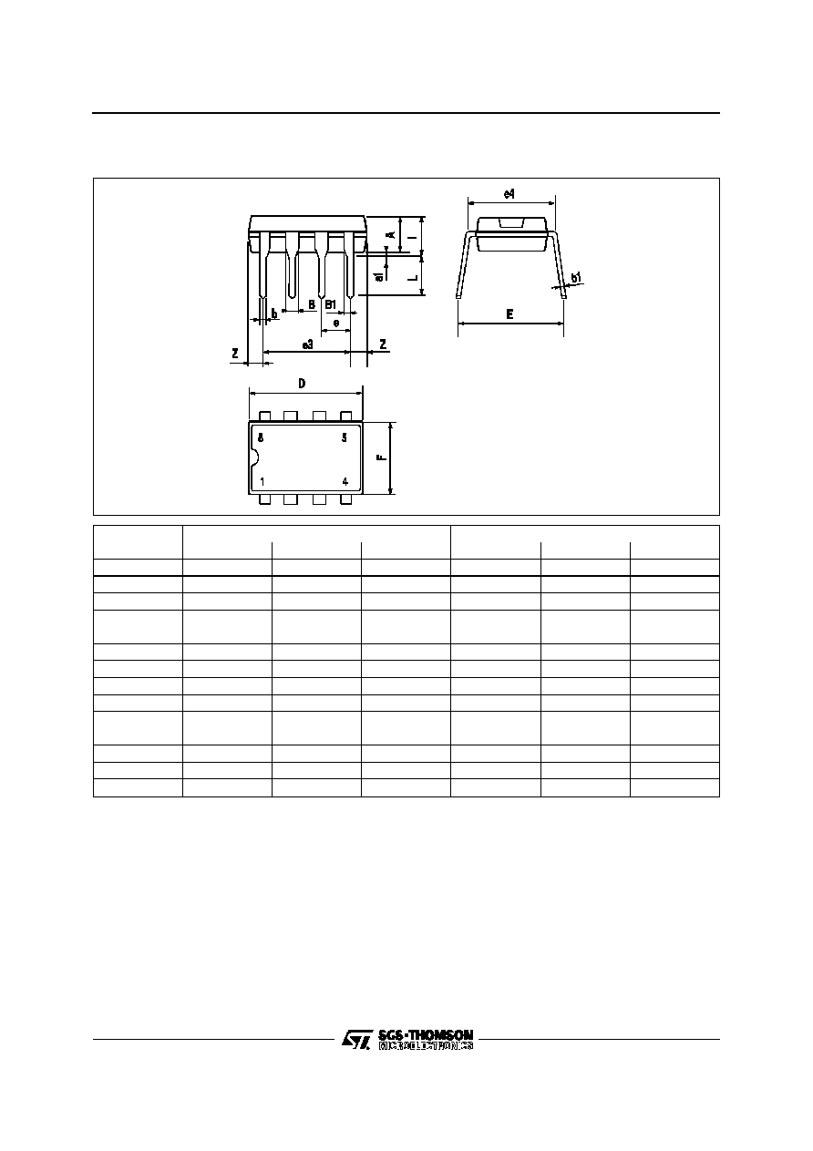
PM-DIP8.EPS
PACKAGE MECHANICAL DATA
8 PINS - PLASTIC DIP
Dimensions
Millimeters
Inches
Min.
Typ.
Max.
Min.
Typ.
Max.
A
3.32
0.131
a1
0.51
0.020
B
1.15
1.65
0.045
0.065
b
0.356
0.55
0.014
0.022
b1
0.204
0.304
0.008
0.012
D
10.92
0.430
E
7.95
9.75
0.313
0.384
e
2.54
0.100
e3
7.62
0.300
e4
7.62
0.300
F
6.6
0260
I
5.08
0.200
L
3.18
3.81
0.125
0.150
Z
1.52
0.060
DIP8.TBL
Information furnished is believed to be accurate and reliable. However, SGS-THOMSON Microelectronics assumes no responsibility
for the consequences of use of such information nor for any infringement of patents or other rights of third parties which may result
from its use. No licence is granted by implication or otherwise under any patent or patent rights of SGS-THOMSON Microelectronics.
Specifications mentioned in this publication are subject to change without noti ce. This publication supersedes and replaces all
information previously supplied. SGS-THOMSON Microelectronics products are not authorized for use as critical components in life
support devices or systems without express written approval of SGS-THOMSON Microelectronics.
©
1996 SGS-THOMSON Microelectronics - All Rights Reserved
Purchase of I
2
C Components of SGS-THOMSON Microelectronics, conveys a license under the Philips
I
2
C Patent. Rights to use these components in a I
2
C system, is granted provided that the system confo rms to
the I
2
C Standard Specifications as defined by Philips.
SGS-THOMSON Microelectronics GROUP OF COMPANIES
Australia - Brazil - Canada - China - France - Germany - Hong Kong - Italy - Japan - Korea - Malaysia - Malta - Morocco
The Netherlands - Singapore - Spain - Sweden - Switzerland - Taiwan - Thailand - United Kingdom - U.S.A.
TDA8196
5/5