
TDA8204B
NICAM DECODER
November 1994
1
2
3
4
5
6
7
8
9
10
11
12
42
41
40
39
38
37
36
35
34
33
32
31
30
29
28
27
26
25
13
14
15
16
17
18
19
20
21
24
23
22
GND
DACDR
DACDL
SERI
RSW
HA0
US2
US1
US0
SCL
SDA
SD
SCK
WS
C4
C3
C2
C1
V
DD
V
DD
V
DD
CK11648
CK728
NDI
GND
TEST
SEL0
SEL1
DV
ADV
PDV
FID
DDO
DDI
GND
MUTE
RESET
ER
GND
TEST0
TEST2
TEST1
82
04B
-
0
1
.
E
P
S
PIN CONNECTIONS
SHRINK 42
(Plastic Package)
ORDER CODE : TDA8204B
.
HIGHLY INTEGRATED TWO-CHIP SOLU-
TION FOR NICAM DEMODULATION (using
TDA8205 QSPK)
.
DATA AND SOUND RECOVERY ACCORDING
TO EBU SPB 424 SPECIFICATIONS
.
I
2
S INTERFACE FOR DIGITAL AUDIO PUR-
POSES (14-bit samples, 32kHz word select
clock, 896kHz serial clock)
.
4 TIMES UP SAMPLING DIGITAL FILTER
AND NOISE SHAPER
.
I
2
C INTERFACE FOR MICROCONTROLLER
SOFTWARE DRIVE
.
PAY TV APPLICATION CAPABILITIES
.
AUTOMATIC ERROR MONITORING
(programmable error rate limit)
DESCRIPTION
The TDA8204B performs two main functions, first
one is NICAM decoding, second one is audio signal
recovery (DAC) combined with audio signal switch-
ing (Matrix). An I
2
S output is provided for digital
audio when required and all functions of both the
TDA8204B and the TDA8205 are accessed via an
on-chip I
2
C bus interface. The I
2
S interface can be
used as an input for converting to analog some I
2
S
digital sound.
1/12
PIN ASSIGMENT
Pin N
o
PIn Name
Function
Pin N
o
Pin Name
Function
1
GND
Ground
22
GND
Ground
2
DACDR
PWM Data Output Right
23
ER
Error Monitor Flag Output
3
DACDL
PWM Data Output Left
24
RESET
Reset
4
SERI
Inter Chip Serial Bus Output
25
MUTE
NICAM Mute
5
V
DD
+5V Supply
26
GND
Ground
6
RSW
Reserve Sound Switch
Status/Control
27
DDI
Descrambled Data Input
7
HA0
Hardware Address Selection
28
DDO
Descrambled Data Output
8
TEST0
To be connected to V
DD
or GND
29
FID
Frame Identification Flag Output
9
US2
User bit 2 (input)
30
PDV
Parity Data Valid Flag Output
10
US1
User bit 1 (output)
31
ADV
Additional Data Valid Flag Output
11
US0
User bit 0 (output)
32
V
DD
+5V Supply
12
SCL
I
2
C Bus Clock
33
DV
Data Valid Flag Output
13
SDA
I
2
C Bus Data
34
SEL1
Language Selection 1 Input
14
SD
I
2
S Bus Data
35
SEL0
Language Selection 0 Input
15
SCK
I
2
S Bus Clock
36
TEST1
Not to be connected
16
WS
I
2
S Bus Word Select
37
TEST
To be connected to GND
17
V
DD
+5V Supply
38
GND
Ground
18
C4
Application Control Bit 4 Flag
39
NDI
NICAM Data Input
19
C3
Application Control Bit 3 Flag
40
CK728
728kHz bit Clock Output
20
C2
Application Control Bit 2 Flag
41
TEST2
Not to be connected
21
C1
Application Control Bit 1 Flag
42
CK11648
11.648MHz bit Clock Input
82
04
B
-
0
1
.
T
B
L
24
14
15
16
34
35
4
7
8
9
10
11
2
3
12
13
18
19
20
21
25
30
37
6
27
28
31
33
40
42
SERIAL
BUS
DIGITAL
FILTER
I C INTERFACE
I S
NOISE
FILTER
2
2
RESET
CK728
CK11648
DACDL
DACDR
SCL
SDA
SE
L
0
SE
L
1
SERI
V
DD
ND
I
DD
O
DD
I
RS
W
ADV
DV
FI
D
ER
WS
SD
US0
US1
HA0
TE
S
T
1
MU
T
E
PD
V
C1
C2
C3
C4
23
29
41 36
SCK
US2
TES
T
0
GN
D
1
22
26 38
5
17
32
NICAM DECODER
39
TE
S
T
2
TE
ST
V
DD
V
DD
GN
D
GN
D
GN
D
8
2
0
4
B-0
2
.
EPS
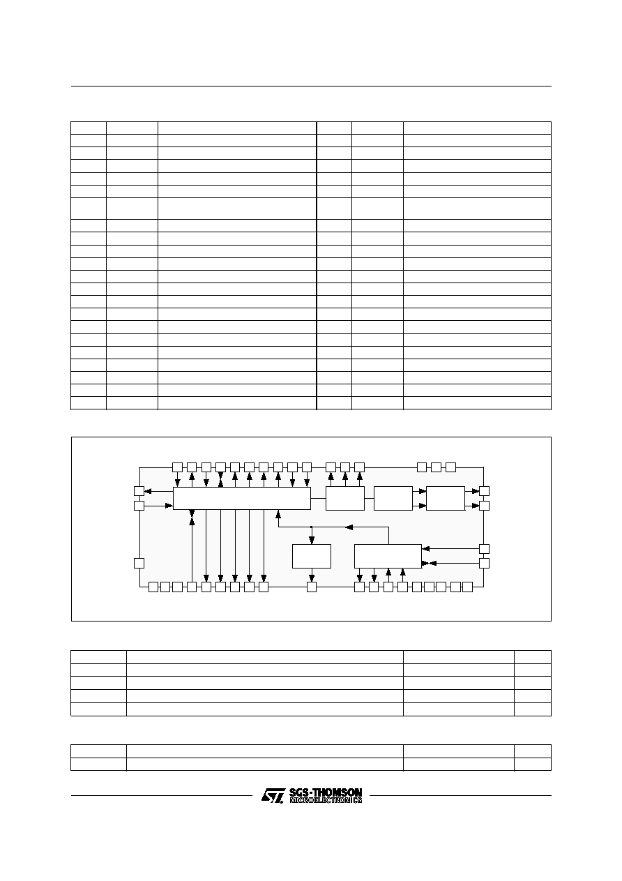
BLOCK DIAGRAM
ABSOLUTE MAXIMUM RATINGS
Symbol
Parameter
Value
Unit
V
DD
Supply Voltage
7
V
P
tot
Total Power Dissipation
1.2
W
T
oper
Operating Temperature Range
0, + 70
o
C
T
stg
Storage Temperature Range
- 20, + 150
o
C
82
04
B
-
0
2
.
T
B
L
THERMAL DATA
Symbol
Parameter
Value
Unit
R
th (j-a)
Thermal Resistance Juntion-ambient
Max.
67
o
C/W
82
04
B
-
0
3.
T
B
L
TDA8204B
2/12

ELECTRICAL CHARACTERISTICS (T
amb
= 25
o
C, V
DD
= 5V, unless otherwise specified)
Symbol
Parameter
Min.
Typ.
Max.
Unit
SUPPLY
V
DD
Supply Voltage Range
4.75
5
5.25
V
I
DD
Supply Current
30
45
90
mA
OUTPUTS
DACDR, DACDL, SERI, US1, SCK, WS, C4, ER, DDO, FID, PDV, ADV, DV, CK728
V
OL
Low Output Voltage (I
OL
= -4mA)
0.4
V
V
OH
High Output Voltage (I
OH
= 4mA)
0.7 V
DD
V
US0 (open drain)
V
OL
Low Output Voltage (I
OL
= -4mA)
0.4
V
I
LK
High Output Current (leakage)
�
2
�
A
CONSTANT CURRENT LED DRIVERS C1, C2, C3
I
OL
Low Output Current (V
OL
= 0.4V)
- 10
mA
INPUTS
HA0, US2, RESET, DDI, SEL1, SEL0, TEST, NDI, CK11
V
IL
Low Input Voltage
0.8
V
V
IH
High Input Voltage
0.6 V
DD
V
I
LK
Input Leakage Current
�
2
�
A
BI-DIRECTIONAL
RSW, MUTE
V
OL
Low Output Voltage (I
OL
= -4mA)
0.4
V
V
OH
High OUtput Voltage (I
OH
= 100
�
A)
0.7 V
DD
V
V
IL
Low Input Voltage
0.8
V
SD
V
OL
Low Output Voltage (I
OL
= -4mA)
0.4
V
V
OH
High Output Voltage (I
OH
= 4mA)
0.7 V
DD
V
V
IL
Low Input Voltage
0.8
V
V
IH
High Input Voltage
0.6 V
DD
V
I
LK
Input Leakage Current
�
2
�
A
I
2
C INTERFACE
SCL
V
IL
Low Input Voltage
0
1.5
V
V
IH
High Input Voltage
3
V
DD
V
f
SCL
SCL Clock Frequency
100
kHz
t
r
, t
f
Input Rise and Fall Times
2
�
s
I
IL
Input Leakage Current (V
I
= 5.5V)
10
�
A
C
I
Input Capacitance
7
pF
SDA
V
IL
Input Low Voltage
0
1.5
V
V
IH
Input High Voltage
3
V
DD
V
t
r
, t
f
Input Rise / Fall Times
2
�
s
I
IL
Input Leakage Current (V
I
= 5.5V with output off)
10
�
A
C
I
Input Capacitance
7
pF
V
OL
Low Output Voltage (I
OL
= 3mA)
0
0.5
V
t
f
Output Fall Time between 3.0V and 1.0V
200
ns
C
I
Load Capacitance
400
pF
82
04
B
-
0
4.
T
B
L
TDA8204B
3/12

ELECTRICAL CHARACTERISTICS (continued)
Symbol
Parameter
Min.
Typ.
Max.
Unit
I
2
C BUS TIMING
SERIAL BUS (referred to V
IH
= 3V, V
IL
= 1.5V)
t
LOW
t
HIGH
Low Period Clock
High Period Clock
4
4
�
s
�
s
t
SU
, d
AT
Data Set-up Time
250
ns
t
HD
, d
AT
Data Hold Time
170
ns
t
SU
, S
TO
Stop Set-up Time from Clock High
4
�
s
t
BUF
Start Set-up Time following a Stop
4
�
s
t
HD
, S
TA
Start Hold Time
4
�
s
t
SU
, S
TA
Start Set-up Time following Clock Low to High Transition
4
�
s
82
04
B
-
0
5
.
T
B
L
SDA
SCL
SDA
t
F
t
BUF
t
LOW
t
HIGH
t
HD, STA
t
r
t
HD, DAT
t
SU, STA
t
SU, STO
t
SU, DAT
V
IH
= 3V, V
IL
= 1.5V
82
04
B
-
0
3
.
E
P
S
Figure 1 : I
2
C Serial Bus Timing
MSB
MSB
word n - 1
right channel
f = 32 kHz
f = 896kHz
CLOCK
WS
SD OUT
word n
left channel
14 bits
word n + 1
right channel
14 bits
LSB
LSB
MSB
MSB
LSB
SD IN
2
I S
8
2
0
4
B-0
4
.
EPS
Figure 2 : I
2
S Bus Timing Diagram
TDA8204B
4/12

CONCEAL
AND MUTE
ERROR
COUNTER
EXPANDER
SCALE FACTOR
RECOVERY
ADDRESS
GENERATOR
3 PAGE
RAM
DESCRAMBLER
MAJORITY
LOGIC
21 20 19 18 6
27
28
39
23
ER
TO FILTER
MUT
E
NDI
PDV
DV
FID
ADV
C1
C2
C3
C4
DD
O
DDI
RSW
30
33
29
31
FRAME
CONTROL
25
82
04
B
-
0
5
.
E
P
S
Figure 3 : NICAM Decoder Block Diagram
FUNCTION DESCRIPTION
The TDA8204B is partitioned into 6 major parts
shown in the block diagram.
The NICAM Decoder performs data and sound
r e c o v e r y f r o m t h e s i g na l s s p e c i f ie d in
EBU SPB 424. The expanded digital audio signals
(14-bit) are made available at the digital audio
interface (I
2
S) in a serial multiplex of left and right
channels. They are also processed by a 4 times
upsampling digital filter and noise shaper which
results in a high speed digital data stream at the
output pins DACDL/DACDR. This data stream can
be applied to the 1-bit D-A convertors contained in
the TDA8205.
The TDA8204B is I
2
C bus controlled and provides
control over the functions of the TDA8205 by
means of a serial inter-chip bus.
1 - NICAM Decoder
1.1 - BLOCK DIAGRAM (see Figure 3)
1.2 - DESCRIPTION
NICAM frame alignment requires searching out a
frame alignment word (FAW) and a 16 frame se-
quence conveyed by C0 bit. Because of noise,
interferences, errors in the incoming NICAM Data,
aliases of the FAW, a robust scheme is imple-
mented. It ensures the decoder will align, and stay
aligned, to signals beyond the limit of maximum
useable error rate. Thanks to a 511 bit PRBS syn-
chronized by the recovered clock and a modulo 2
adder, original data are recovered. This data
stream can be processed externaly for de-encryp-
tion in Pay TV applications using descrambled data
Pins DDO, DDI.
To allow simultaneous reading and writing of
mono/stereo samples, de-interleaved data frames
are stored in a 3 page RAM.
The 10-bit input audio samples are expanded to
14-bit using scale factor bits according to NICAM
decoding rules. Samples in error by the parity
check are replaced by interpolated one or re-
peated.
Mute is set according to an error counter when the
error rate exceeds error rate limit (ERL) and reset
when the error rate is below ERL/4.
Application control information (bit C1, C2, C3, C4)
is recovered by majority decision logic over 16
frames. the C1, C2, C3 , C4 bits can be read in SR0
register and are set on the C1, C2, C3, C4 pins
according to the state of bit 0 (BEA) of the CR2
register.
2 - Digital Filter and Noise Shaper
A digital filter performs 4X upsampling in two
stages. The main FIR 2x upsampler is followed by
a smaller 2x FIR upsampler. Digital upsampling
means a much simpler post-DAC reconstruction
filter can be used thus saving on external compo-
nent count and cost.
A noise shaper converts the samples from the
digital filter into two high speed serial bitstreams
which can be applied to the DACs in the TDA8205.
3 - I
2
S Bus
A standard three-wire interface, conforming to the
I
2
S bus protocol, is provided, allowing connection
of an external DAC or DAT interface. Audio samples
contain 14-bit, so 16-bit DACs will pad the two LSBs
with 0. The word select clock operates at 32kHz
and the serial clock at 896kHz.
By setting SDI bit of CR2 to 1, the I
2
S interface can
receive the digital I
2
S sound. This prevents dupli-
cating the dual D/A converter.
TDA8204B
5/12