
Application Specific Discretes
A.S.D.
TM
THDT6511D
DUALASYMETRICALTRANSIENTSUPPRESSOR
PEAK PULSE CURRENT : I
PP
= 40A, 10/100
µ
s
HOLDING CURRENT : 150 mA min.
BREAKDOWN VOLTAGE : 65 V min.
LOW DYNAMIC CHARACTERISTICS
STAND CCITT K20 AND LSSGR
FEATURES
SO8
This device has been especially designed to
protect subscriber line cards against overvoltage.
Two diodes clamp positive overloads while
negative surges are suppressed by two protection
thyristors.
A particular attention has been given to the internal
wire bonding. The "4-point" configuration ensures
a reliable protection, eliminating overvoltages
introduced by the parasitic inductances of the
wiring (Ldi/dt), especially for very fast transient
overvoltages.
DESCRIPTION
GND
GND
TIP
TIP
RING
RING
1
2
3
4
5
6
7
8
GND
GND
SCHEMATIC DIAGRAM
TRANSIENT VOLTAGE SUPPRESSOR
FOR SLIC PROTECTION
PRELIMINARY DATASHEET
February 1998 - Ed: 2
CCITT K20 :
10/700
µ
s
1kV
5/310
µ
s
38A
VDE 0433 :
10/700
µ
s
2kV
5/310
µ
s
50A
VDE 0878 :
1.2/50
µ
s
1.5kV
1/20
µ
s
40A
I3124 :
0.5/700
µ
s
1kV
0.2/310
µ
s
38A
FCC part 68 :
2/10
µ
s
2.5kV
2/10
µ
s
125A (*)
BELLCORE
TR-NWT-001089 :
2/10
µ
s
2.5kV
2/10
µ
s
125A (*)
10/1000
µ
s
1kV
10/1000
µ
s
40A (*)
(*) with series resistors or PTC.
COMPLIESWITH THE FOLLOWINGSTANDARDS :
1/6
Symbol
Parameter
Value
Unit
I
PP
Peak pulse current
(see note 1)
10/1000
µ
s
5/310
µ
s
2/10
µ
s
40
50
125
A
I
TSM
Non repetitive surge peak on-state current
F = 50 Hz
t = 300 ms
t = 1 s
t = 5 s
10
3.5
1
A
I
TSM
F = 50 Hz, 60 x 1 s, 2 mn between pulse
1
A
T
stg
T
j
Storage temperature range
Maximum junction temperature
- 55 to + 150
150
∞
C
T
L
Maximum lead temperature for soldering during 10s
260
∞
C
ABSOLUTE MAXIMUM RATINGS (T
amb
= 25
∞
C)
Note 1 : Pulse waveform :
10/1000
µ
s
tr=10
µ
s
tp=1000
µ
s
5/310
µ
s
tr=5
µ
s
tp=310
µ
s
2/10
µ
s
tr=2
µ
s
tp=10
µ
s
100
50
% I
PP
t
t
r
p
0
t
Symbol
Parameter
Value
Unit
R
th (j-a)
Junction to ambient
170
∞
C/W
THERMAL RESISTANCES
I
I
F
V
BO
V
RM
I
RM
V
F
V
I
pp
I
H
I
BO
V
BR
Symbol
Parameter
V
RM
Stand-off voltage
I
RM
Leakagecurrent at stand-offvoltage
V
BR
Breakdown voltage
V
BO
Breakover voltage
I
H
Holding current
V
F
Forward voltage drop
V
FP
Peak forward voltage
I
BO
Breakover current
I
PP
Peak pulse current
C
Capacitance
T
Temperature coefficient
ELECTRICAL CHARACTERISTICS
(T
amb
= 25
∞
C)
THDT6511D
2/6

Symbol
Tests conditions
Min.
Typ.
Max.
Unit
V
BR
I
R
= 1mA
65
V
V
BO
68
85
V
I
RM
V
RM
= 63 V
100
µ
A
I
BO
tp = 100
µ
s
110
450
mA
I
BO
F = 50 Hz
RG = 600
500
mA
I
H
150
mA
T
15
10
-4
/
∞
C
C
V
D
= 100 mV
RMS
F = 1KHz
500
pF
dV/dt
Linear ramp up to 67 % of V
BR
5
kV /
µ
s
2 - PARAMETERS RELATED TO PROTECTION THYRISTOR
Symbol
Test conditions
Min.
Typ.
Max.
Unit
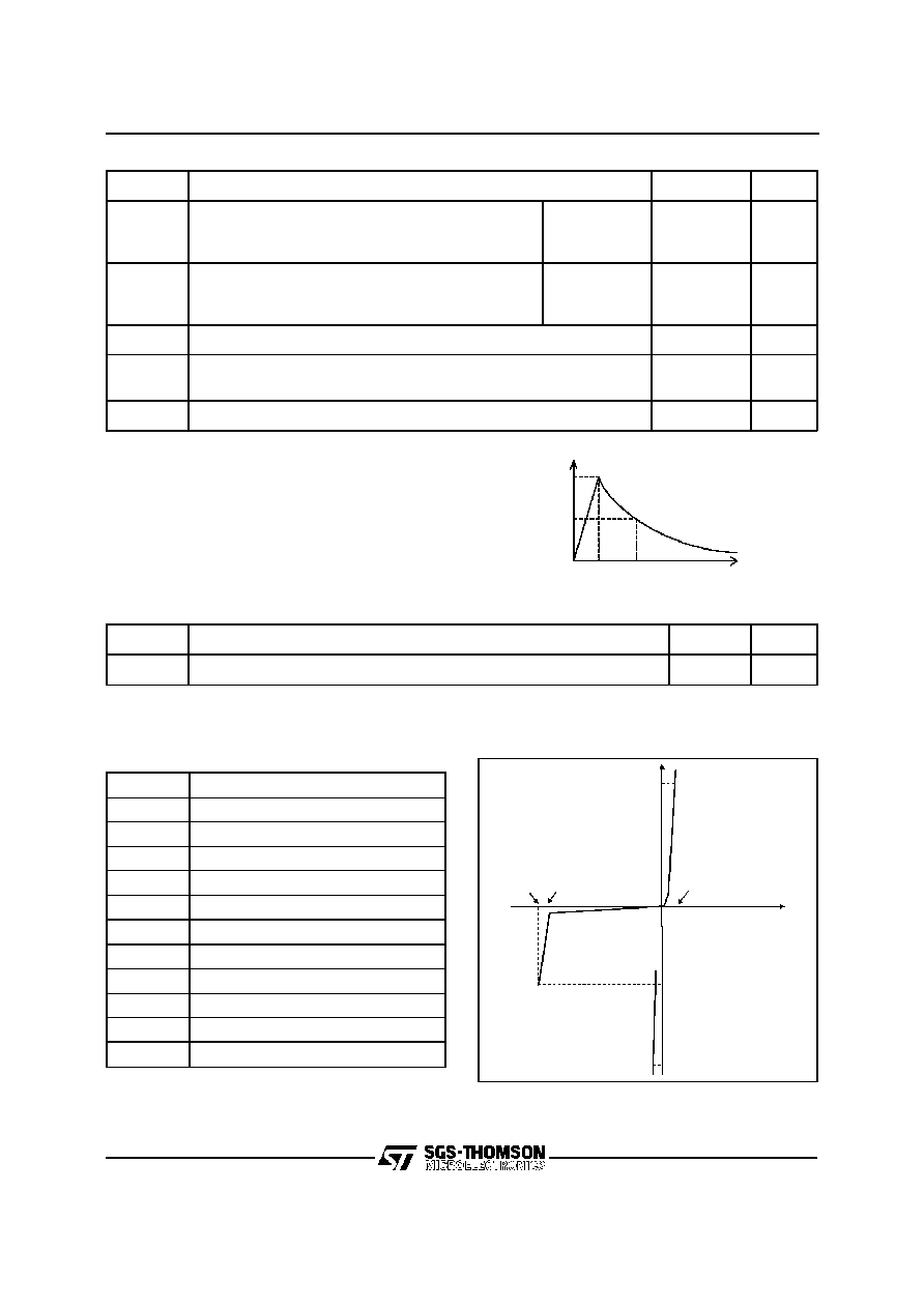
V
F
I
F
= 1 A
tp = 100
µ
s
2
V
V
FP
see curve fig. 1
NA
NA
NA
V
NA : Non Available
1 - PARAMETERS RELATED TO DIODE LINE / GND
THDT6511D
3/6
DYNAMIC CHARACTERISTICS : V
FP
and V
BO
Figure 1 :
60
10
5
2
-85
-100
-130
250 ns
10 us
10 ms
1 us
200 ns
t
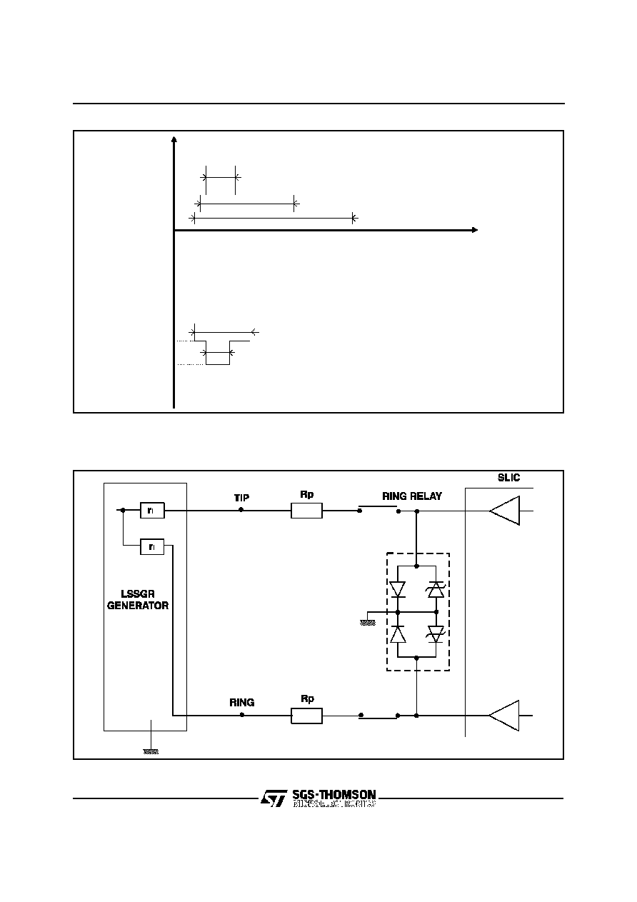
LSSGR TEST DIAGRAM
Figure 2 :
THDT6511D
Under lightning and power crossing test, the device limits the transient voltage to the values
indicated in the figure
To stand the LSSGR test requirements, Rp must be
15
THDT6511D
4/6

RING
RELAY
RING
GENERATOR
PTC
PTC
LINE A
LINE B
- V
Integrated
SLIC
T
E
S
T
R
E
L
A
Y
bat
THBT200S
TIP
RING
THDT651 D
1
TYPICAL APPLICATION
P1
D1
Line A
Line B
Tip
Ring
- For positive surges versus GND (TIP), diode D
1
will conduct.
- For negative surges versus GND (TIP),
protection device P
1
will trigger at maximum
voltage equal to V
BO
.
THDT6511D
5/6