 | –≠–ª–µ–∫—Ç—Ä–æ–Ω–Ω—ã–π –∫–æ–º–ø–æ–Ω–µ–Ω—Ç: TPA62 | –°–∫–∞—á–∞—Ç—å:  PDF PDF  ZIP ZIP |

TPA SERIES
BIDIRECTIONAL CROWBAR PROTECTION.
VOLTAGE RANGE: FROM 62 V TO 270 V.
HOLDING CURRENT :
I
H
= 150mA min.
REPETITIVE PEAK PULSE CURRENT :
I
PP
= 50 A, 10/1000
µ
s.
FEATURES
F126
The TPA series are TRISIL devices especially de-
signed for protecting sensitive telecommunication
equipment against lightning and transient voltages
induced by AC power lines. They are available in
the F126 axial package.
TRISIL devices provide bidirectional protection
by crowbar action. Their characteristic response
to transient overvoltages makes them particularly
suited to protect voltage sensitive telecommuni-
cation equipment.
DESCRIPTION
SCHEMATIC DIAGRAM
TRISIL
TM
COMPLIES WITH THE
FOLLOWING STANDARDS:
Peak Surge
Voltage
(V)
Voltage
Waveform
(
µ
s)
Current
Waveform
(
µ
s)
Admissible
Ipp
(A)
Necessary
Resistor
(
)
(CCITT) ITU-K20
1000
10/700
5/310
25
-
(CCITT) ITU-K17
1500
10/700
5/310
38
-
VDE0433
2000
10/700
5/310
50
-
VDE0878
2000
1.2/50
1/20
50
-
IEC-1000-4-5
level 3
level 4
10/700
1.2/50
5/310
8/20
50
100
-
-
FCC Part 68, lightning surge
type A
1500
800
10/160
10/560
10/160
10/560
75
55
12.5
6.5
FCC Part 68, lightning surge
type B
1000
9/720
5/320
25
-
BELLCORE TR-NWT-001089
First level
2500
1000
2/10
10/1000
2/10
10/1000
150
50
11.5
10
BELLCORE TR-NWT-001089
Second level
5000
2/10
2/10
150
11.5
CNET l31-24
1000
0.5/700
0.8/310
25
-
Æ
October 1998 - Ed: 9A
1/5

Symbol
Parameter
V
RM
Stand-off voltage
I
RM
Leakage current at stand-off voltage
V
R
Continuous Reverse voltage
V
BR
Breakdown voltage
V
BO
Breakover voltage
I
H
Holding current
I
BO
Breakover current
I
PP
Peak pulse current
C
Capacitance
ELECTRICAL CHARACTERISTICS
(T
amb
= 25
∞
C)
Symbol
Parameter
Value
Unit
R
th
(j-l)
Junction to leads (L
lead
= 10mm)
60
∞
C/W
R
th
(j-a)
Junction to ambient on printed circuit (L
lead
= 10 mm)
100
∞
C/W
THERMAL RESISTANCES
Note 1:
I
R
measured at V
R
guarantee V
BRmin
V
R
Note 2:
Measured at 50 Hz (1 cycle) - See test circuit 1.
Note 3:
See test circuit 2.
Note 4:
V
R
= 1V, F = 1MHz. Refer to fig.3 for C versus V
R
.
Type
I
RM
@ V
RM
I
R
@ V
R
V
BO
@ I
BO
I
H
C
max.
max.
note 1
max.
note 2
min.
note 3
max.
note 4
µ
A
V
µ
A
V
V
mA
mA
pF
TPA62
TPA68
TPA100
TPA120
TPA130
TPA180
TPA200
TPA220
TPA240
TPA270
2
2
2
2
2
2
2
2
2
2
56
61
90
108
117
162
180
198
216
243
50
50
50
50
50
50
50
50
50
50
62
68
100
120
130
180
200
220
240
270
82
90
133
160
173
240
267
293
320
360
800
800
800
800
800
800
800
800
800
800
150
150
150
150
150
150
150
150
150
150
150
150
100
100
100
100
100
100
100
100
Symbol
Parameter
Value
Unit
P
Power dissipation on infinite heatsink
T
amb
= 50
∞
C
1.7
W
I
PP
Peak pulse current
10/1000
µ
s
8/20
µ
s
50
100
A
I
TSM
Non repetitive surge peak on-state current
tp = 20 ms
30
A
I
2
t
I
2
t value for fusing
tp = 20 ms
9
A
2
s
dV/dt
Critical rate of rise of off-state voltage
V
RM
5
kV/
µ
s
T
stg
T
j
Storage temperature range
Maximum junction temperature
- 55 to + 150
150
∞
C
∞
C
T
L
Maximum lead temperaturefor solderingduring 10s at 5mm from case
230
∞
C
ABSOLUTE MAXIMUM RATINGS (T
amb
= 25
∞
C)
TPA SERIES
2/5

TEST CIRCUIT 1 FOR I
BO
and V
BO
parameters:
22
0V
static
relay.
R1
R2
240
140
D.U.T
V BO
measure
IBO
measure
tp = 20ms
K
Transformer
220V/800V
5A
Auto
Transformer
220V/2A
Vout
TEST PROCEDURE :
Pulse Test duration (tp = 20ms):
- For Bidirectional devices = Switch K is closed
- For Unidirectional devices = Switch K is open.
V
OUT
Selection
- Device with V
BO
<
200 Volt
- V
OUT
= 250 V
RMS
, R
1
= 140
.
- Device with V
BO
200 Volt
- V
OUT
= 480 V
RMS
, R
2
= 240
.
TEST CIRCUIT 2 for I
H
parameter.
R
- V
P
V
BAT
= - 48 V
Surge generator
D.U.T.
This is a GO-NOGO Test which allows to confirm the holding current (I
H
) level in a functional
test circuit.
TEST PROCEDURE :
1) Adjust the current level at the I
H
value by short circuiting the AK of the D.U.T.
2) Fire the D.U.T with a surge Current : Ipp = 10A , 10/1000
µ
s.
3) The D.U.T will come back off-state within 50 ms max.
TPA SERIES
3/5

TSM
(A)
Fig. 1: Non repetitive surge peak on-state current
versus overload duration (Tj initial=25
∞
C).
Fig. 2: Relative variation of holding current versus
junction temperature.
tp(s)
Fig. 5: Transient thermal impedance junction to
ambient versus pulse duration (for FR4 PC Board
with T
lead
= 10 mm).
V (V)
R
Fig. 3: Relative variation of junction capacitance
versus reverse applied voltage (typical values).
Note: For V
RM
upper than 56V, the curve is
extrapolated(dotted line).
I (A)
T
V (V)
T
Fig. 4: On-state current versus on-state voltage
(typical values).
TPA SERIES
4/5
ORDER CODE
TPA
100
RL
VOLTAGE
PACKAGING:
RL = tape and reel.
= Ammopack.
TRISIL PROTECTION 50A
Packaging : Standard packaging is in tape and reel.
MARKING :
Logo, Date Code, Part Number.
Information furnished is believed to be accurate and reliable. However, STMicroelectronics assumes no responsIbility for the consequences of
use of such information nor for any infringement of patents or other rights of third parties which may result from its use. No license is granted by
implication or otherwise under any patent or patent rights of STMicroelectronics. Specifications mentioned in this publication are subject to
change without notice. This publication supersedes and replaces all information previously supplied.
STMicroelectronics products are not authorized for use as critical components in life support devices or systems without express written ap-
proval of STMicroelectronics.
The ST logo is a registered trademark of STMicroelectronics
©
1998 STMicroelectronics - Printed in Italy - All rights reserved.
STMicroelectronics GROUP OF COMPANIES
Australia - Brazil - Canada - China - France - Germany - Italy - Japan - Korea - Malaysia - Malta - Mexico - Morocco -
The Netherlands - Singapore - Spain - Sweden - Switzerland - Taiwan - Thailand - United Kingdom - U.S.A.
http://www.st.com
Weight: 0.40 g
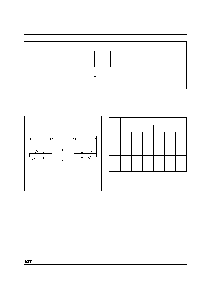
PACKAGE MECHANICAL DATA
F126 Plastic
A
C
C
D
D
B
REF.
DIMENSIONS
Millimeters
Inches
Min.
Typ.
Max.
Min.
Typ.
Max.
A
6.05
6.20
6.35 0.238 0.244 0.250
B
2.95
3.00
3.05 0.116 0.118 0.120
C
26
31
1.024
1.220
D
0.76
0.81
0.86 0.030 0.032 0.034
TPA SERIES
5/5