 | –≠–ª–µ–∫—Ç—Ä–æ–Ω–Ω—ã–π –∫–æ–º–ø–æ–Ω–µ–Ω—Ç: TSM104W | –°–∫–∞—á–∞—Ç—å:  PDF PDF  ZIP ZIP |

1/9
OPERATIONAL AMPLIFIERS
s
LOW SUPPLY CURRENT : 375
µ
A/op.
(@ V
CC
= 5V)
s
LOW INPUT BIAS CURRENT : 20nA
s
MEDIUM SPEED : 0.9MHz
s
LOW INPUT OFFSET VOLTAGE : 0.5mV typ
for TSM104WA
s
WIDE POWER SUPPLY RANGE : ±1.5V to
±15V
s
2kV ESD PROTECTION
VOLTAGE REFERENCE
s
ADJUSTABLE OUTPUT VOLTAGE :
V
ref
to 36V
s
0.4% AND 1% VOLTAGE PRECISION
s
SINK CURRENT CAPABILITY : 1 to 100mA
s
TYPICAL OUTPUT IMPEDANCE : 0.2
DESCRIPTION
The TSM104W is a monolithic IC that includes
four op-amps and an adjustable shunt voltage ref-
erence. This device is offering space and cost
saving in many applications like power supply
management or data acquisition systems.
ORDER CODE
N = Dual in Line Package (DIP)
D = Small Outline Package (SO) - also available in Tape & Reel (DT)
PIN CONNECTIONS (top view)
Part Number Temperature Range
Package
N
D
TSM104WI/AI
-40∞C, +105∞C
∑
∑
N
DIP16
(Plastic Package)
D
SO16
(Plastic Micropackage)
1
2
3
4
13
14
15
16
5
6
7
8
12
11
10
9
Output 1
Inverting Input 1
Non-inverting Input 1
V
CC
+
Non-inverting Input 2
Inverting Input 2
Output 2
Adjust
Output 4
Inverting Input
Non-inverting Input 4
Non-inverting Input 3
Inverting Input 3
Output 3
Cathode
V
CC
-
TSM104W/A
QUAD OPERATIONAL AMPLIFIER AND
PROGRAMMABLE VOLTAGE REFERENCE
January 2003
TSM104W/A
2/9
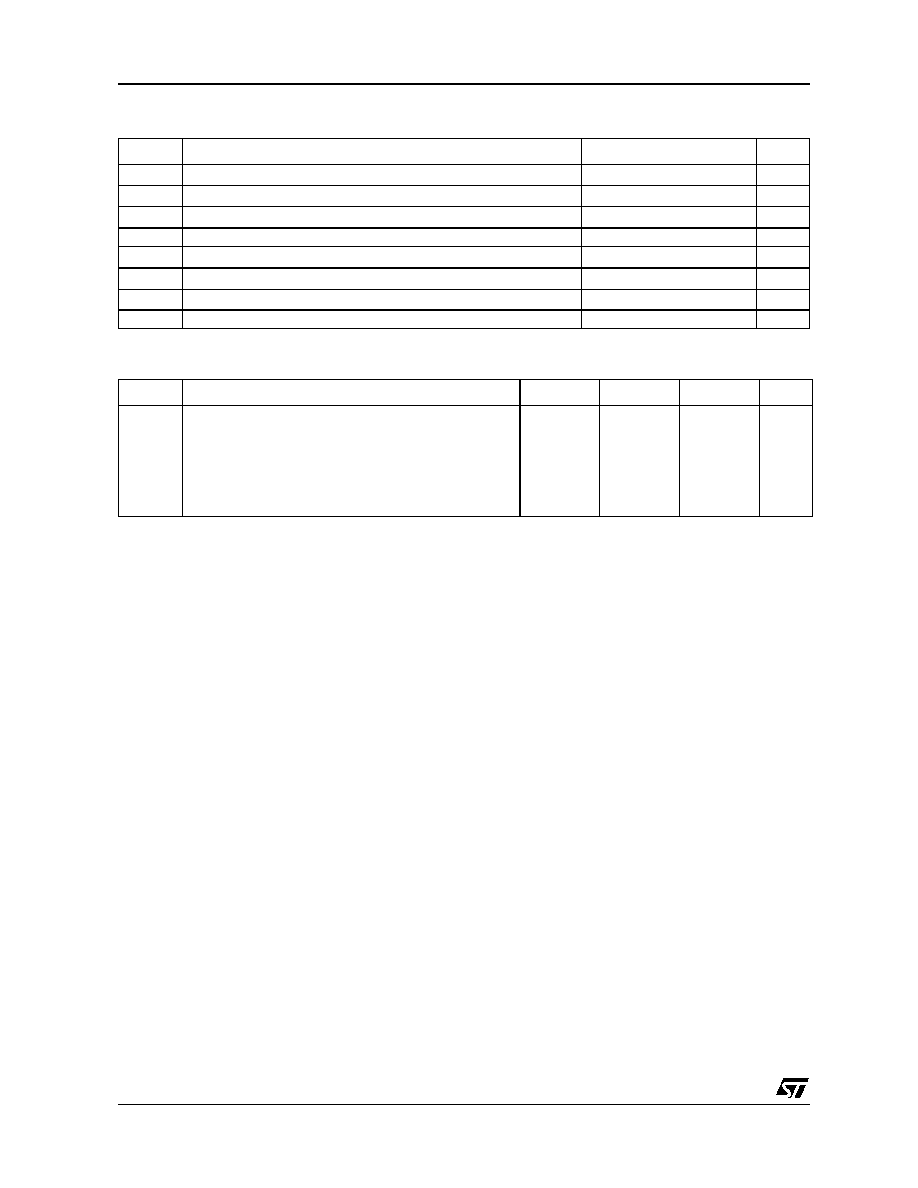
ABSOLUTE MAXIMUM RATINGS
ELECTRICAL CHARACTERISTICS
V
CC
+
= 5V, V
CC
-
= 0V, T
amb
= 25∞C (unless otherwise specified)
Symbol
Parameter
Value
Unit
V
CC
Supply Voltage
36
V
V
id
Differential Input Voltage
36
V
V
i
Input Voltage
-0.3 to Vcc + 0.3
V
Output Short-circuit Duration
Infinite
T
oper
Operating Free-Air Temperature Range
-55 to +125
∞C
T
j
Maximum Junction Temperature
150
∞C
R
thja
Thermal Resistance Junction to Ambient (SO package)
150
∞C/W
ESD
Electrostatic Discharge Protection
2
kV
Symbol
Parameter
Min
Typ
Max
Unit
I
CC
Total Supply Current, excluding current in the Voltage
Reference
V
CC
+
= 5V, no load
T
min.
< T
amb
< T
max.
V
CC
+
= 30V, no load
T
min.
< T
amb
< T
max.
1.4
2.4
4
mA

TSM104W/A
3/9
ELECTRICAL CHARACTERISTICS
V
CC
+
= 5V, V
cc
-
= Ground, V
O
= 1.4V, T
amb
= 25∞C (unless otherwise specified)
Symbol
Parameter
Min.
Typ.
Max.
Unit
V
io
Input Offset Voltage
TSM104W, T
amb
= 25∞C
T
min
T
amb
T
max
TSM104WA, T
amb
= 25∞C
T
min
T
amb
T
max
1
0.5
5
6
3
4
mV
V
io
Input Offset Voltage Drift
7
µ
V/∞C
Iio
Input Offset Current
T
min
T
amb
T
max
2
30
50
nA
I
ib
Input Bias Current
T
min
T
amb
T
max
20
150
200
nA
A
vd
Large Signal Voltage Gain
V
CC
= 15V, R
L
= 2k
V
O
= 1.4V to 11.4V
T
min
T
amb
T
max
50
25
100
V/mV
SVR
Supply Voltage Rejection Ratio
V
CC
= 5V to 30V
65
100
dB
Vicm
Input Voltage Mode Voltage Range
V
CC
= + 30V see note
1)
T
min
T
amb
T
max
1.
The input common-mode voltage of either input signal voltage should not be allowed to go negative by more than 0.3V. The upper end of the
common-mode voltage range is V
CC
+
-1.5V, but either of both inputs can go to Vcc+0.3V without damage.
0
0
Vcc
+
-1.5
Vcc
+
-2
V
CMR
Common Mode Rejection Ratio
T
min
T
amb
T
max
70
60
85
dB
I
source
Output Current Source
V
o
= 2V, V
cc
= +15V, V
id
= +1V
20
40
mA
I
o
Output Short Circuit to Ground
V
CC
= +15V
40
60
mA
I
sink
Output Current Sink
V
id
= -1V
V
CC
= +15V, V
o
= +2V
10
20
mA
V
OH
High Level Output Voltage
R
L
= 10k, V
CC
+
= 30V
T
amb
= 25∞C
T
min
T
amb
T
max
27
27
28
V
V
OL
Low Level Output Voltage
R
L
= 10k
T
min
T
amb
T
max
5
20
20
mV
SR
Slew Rate at Unity Gain
V
i
= 0.5 to 3V, V
CC
= 15V
R
L
= 2k
, C
L
= 100pF, unity gain
0.1
0.3
V/
µ
s
GBP
Gain Bandwith Product
V
CC
= 30V, R
L
= 2k, C
L
= 100pF
f = 100kHz, V
in
= 10mV
0.5
0.9
MHz
THD
Total Harmonic Distortion
f = 1kHz
A
V
= 20dB, R
L
= 2, V
CC
= 30V
C
L
= 100pF, V
o
= 2Vpp
0.02
%
e
n
Equivalent Input Noise Voltage
f = 1kHz, V
CC
= 30V, R
s
= 100
50
Cs
Channel Separation
1kHz < f < 20kHz
120
dB
nV
Hz
------------
But either of both inputs can go to +36V without damage

TSM104W/A
4/9
VOLTAGE REFERENCE
1) The dynamic impedance is defined as
=
Symbol
Conditions
Value
Unit
I
k
Cathode Current
1 to 100
mA
Symbol
Parameter
Min
Typ
Max
Unit
V
ref
Reference Input Voltage
TSM104W, T
amb
= 25∞C
T
min
T
amb
T
max
TSM104WA, T
amb
= 25∞C
T
min
T
amb
T
max
2.475
2.45
2.49
2.48
2.5
2.5
2.525
2.55
2.51
2.52
V
V
ref
Reference Input Voltage Deviation Over Temperature Range
V
KA
= V
ref
, I
K
= 10mA
T
min
T
amb
T
max
7
30
mV
Ratio of Change in Reference Input Voltage to Charge in
Cathode to Anode Voltage
I
K
= 10mA,
V
KA
=36V to 3V
-2
-1.1
mV/V
I
ref
Reference Input Current
I
K
= 10mA
T
min
T
amb
T
max
1.5
2.5
3
µ
A
I
ref
Reference Input Current Deviation over T∞ Range
0.8
1.2
µ
A
I
min
Minimum Cathode Current for Regulation
V
KA
= V
ref
0.5
1
mA
I
off
Off-State Cathode Current
180
500
nA
Dynamic Impedance - note 1
V
KA
= V
ref
,
I
K
= 1 to 100mA, f < 1kHz
0.2
0.5
V
ref
V
K A
----------------
Z
KA
Z
KA
V
K A
VI
K
----------------

TSM104W/A
5/9
OPERATIONAL AMPLIFIERS
-0.015
-0.01
-0.005
0
0.005
0.01
0.015
source <=
I (A)
=> sink
0
200
400
600
800
1000
T
hous
ands
Un
i
t
F
r
e
q
Unit Frequency = F(I)
Vcc=±15V, RL=2k, CL=100pF
-0.015
-0.01
-0.005
0
0.005
0.01
0.015
source <=
I (A)
=> sink
0
200
400
600
800
T
hous
ands
GB
P
GBP = F(I)
Vcc=±15V, RL=2k, CL=100pF
-0.015
-0.01
-0.005
0
0.005
0.01
0.015
source <=
I (A)
=> sink
0
10
20
30
40
50
60
P
has
e
M
ar
gi
n
(
deg)
-14
-12
-10
-8
-6
-4
-2
0
G
a
i
n
Ma
rg
i
n
(d
B
)
Phase and Gain Margin = F(I)
Vcc=+/-15V, RL=2k, CL=100pF