 | –≠–ª–µ–∫—Ç—Ä–æ–Ω–Ω—ã–π –∫–æ–º–ø–æ–Ω–µ–Ω—Ç: TYN1025 | –°–∫–∞—á–∞—Ç—å:  PDF PDF  ZIP ZIP |

1/7
Æ
TN25 and TYNx25 Series
STANDARD
25A SCRs
April 2002 - Ed: 4A
MAIN FEATURES:
DESCRIPTION
The TYN / TN25 SCR Series is suitable for
general purpose applications.
Using clip assembly technology, they provide a
superior performance in surge current capabilities.
Symbol
Value
Unit
I
T(RMS)
25
A
V
DRM
/V
RRM
600 to 1000
V
I
GT
40
mA
ABSOLUTE RATINGS (limiting values)
Symbol
Parameter
Value
Unit
I
T(RMS)
RMS on-state current (180∞ conduction angle)
Tc = 100∞C
25
A
T
(AV)
Average on-state current (180∞ conduction angle)
Tc = 100∞C
16
A
I
TSM
Non repetitive surge peak on-state
current
tp = 8.3 ms
Tj = 25∞C
314
A
tp = 10 ms
300
I
≤
t
I
≤
t Value for fusing
tp = 10 ms
Tj = 25∞C
450
A
2
S
dI/dt
Critical rate of rise of on-state current
I
G
= 2 x I
GT
, tr
100 ns
F = 60 Hz
Tj = 125∞C
50
A/µs
I
GM
Peak gate current
tp = 20 µs
Tj = 125∞C
4
A
P
G(AV)
Average gate power dissipation
Tj = 125∞C
1
W
T
stg
Tj
Storage junction temperature range
Operating junction temperature range
- 40 to + 150
- 40 to + 125
∞C
V
RGM
Maximum peak reverse gate voltage
5
V
A
K
G
D
2
PAK
(TN25-G)
G
A
A
K
TO-220AB
(TYN)
A
A
G
K

TN25 and TYNx25 Series
2/7
ELECTRICAL CHARACTERISTICS (Tj = 25∞C, unless otherwise specified)
THERMAL RESISTANCES
S = Copper surface under tab
PRODUCT SELECTOR
Symbol
Test Conditions
Value
Unit
I
GT
V
D
= 12 V R
L
= 33
MIN.
4
mA
MAX.
40
V
GT
MAX.
1.3
V
V
GD
V
D
= V
DRM
R
L
= 3.3 k
Tj = 125∞C
MIN.
0.2
V
I
H
I
T
= 500 mA Gate open
MAX.
50
mA
I
L
I
G
= 1.2 I
GT
MAX.
90
mA
dV/dt
V
D
= 67 % V
DRM
Gate open
Tj = 125∞C
MIN.
1000
V/µs
V
TM
I
TM
= 50 A tp = 380 µs
Tj = 25∞C
MAX.
1.6
V
V
t0
Threshold voltage
Tj = 125∞C
MAX.
0.77
V
R
d
Dynamic resistance
Tj = 125∞C
MAX.
14
m
I
DRM
I
RRM
V
DRM
= V
RRM
Tj = 25∞C
MAX.
5
µA
Tj = 125∞C
4
mA
Symbol
Parameter
Value
Unit
R
th(j-c)
Junction to case (DC)
1.0
∞C/W
R
th(j-a)
Junction to ambient (DC)
TO-220AB
60
∞C/W
S = 1 cm
≤
D
≤
PAK
45
Part Number
Voltage (xxx)
Sensitivity
Package
600 V
800 V
1000 V
TN2540-xxxG
X
X
X
40 mA
D
≤
PAK
TYNx25
X
X
X
40 mA
TO-220AB

TN25 and TYNx25 Series
3/7
ORDERING INFORMATION
TN 25 40 - 600 G (-TR)
STANDARD
SCR
SERIES
CURRENT: 25A
SENSITIVITY:
40: 40mA
VOLTAGE:
600: 600V
800: 800V
1000: 1000V
PACKAGE:
G: D PAK
2
PACKING MODE:
Blank: Tube
-TR: Tape & Reel
TYN 6 25 (RG)
CURRENT: 25A
VOLTAGE:
6: 600V
8: 800V
10: 1000V
STANDARD
SCR
SERIES
PACKING MODE
Blank: Bulk
RG: Tube
OTHER INFORMATION
Note: x = voltage
Part Number
Marking
Weight
Base Quantity
Packing mode
TN2540-x00G
TN2540x00G
1.5 g
50
Tube
TN2540-x00G-TR
TN2540x00G
1.5 g
1000
Tape & reel
TYNx25
TYNx25
2.3 g
250
Bulk
TYNx25RG
TYNx25
2.3 g
50
Tube
TN25 and TYNx25 Series
4/7
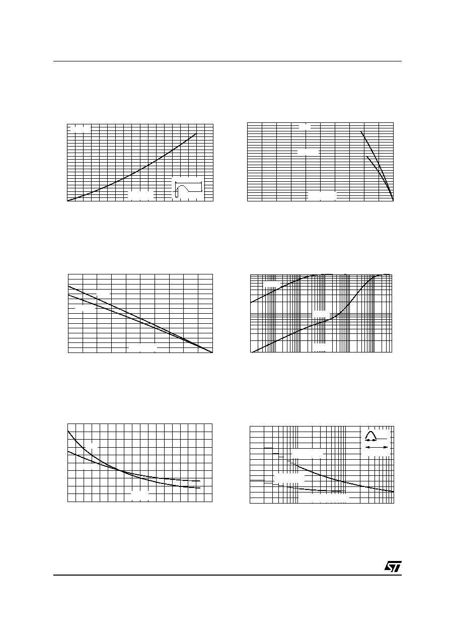
Fig. 1: Maximum average power dissipation
versus average on-state current.
Fig. 2-1: Average and D.C. on-state current
versus case temperature.
Fig. 2-2: Average and D.C. on-state current
versus ambient temperature (copper surface
under tab: S = 1 cm≤ (for D≤PAK).
Fig. 3: Relative variation of thermal impedance
versus pulse duration.
Fig. 4: Relative variation of gate trigger current,
holding current and latching current versus
junction temperature.
Fig. 5: Surge peak on-state current versus
number of cycles.
0
2
4
6
8
10
12
14
16
0
2
4
6
8
10
12
14
16
18
20
22
24
P(W)
= 180∞
IT(av)(A)
360∞
0
25
50
75
100
125
0
2
4
6
8
10
12
14
16
18
20
22
24
26
28
IT(av)(A)
D.C.
= 180∞
Tcase(∞C)
0
25
50
75
100
125
0.0
0.5
1.0
1.5
2.0
2.5
3.0
3.5
4.0
IT(av)(A)
D.C.
= 180∞
Tamb(∞C)
1E-3
1E-2
1E-1
1E+0
1E+1
1E+2 5E+2
0.01
0.10
1.00
K = [Zth/Rth]
Zth(j-c)
Zth(j-a)
tp(s)
-40
-20
0
20
40
60
80
100
120
140
0.0
0.5
1.0
1.5
2.0
2.5
IGT,IH,IL [Tj] / IGT ,IH,IL [Tj = 25 ∞C]
IGT
IH & IL
Tj(∞C)
1
10
100
1000
0
50
100
150
200
250
300
350
ITSM(A)
Non repetitiv e
Tj initial = 25 ∞C
Repetitive
Tcase = 100 ∞C
Number of cycles
One cycle
tp = 10ms

TN25 and TYNx25 Series
5/7
Fig. 6: Non-repetitive surge peak on-state
current for a sinusoidal pulse with width
tp < 10 ms, and corresponding values of I≤t.
Fig. 7: On-state characteristics (maximum
values).
Fig. 8: Thermal resistance junction to ambient
versus copper surface under tab (Epoxy printed
circuit board FR4, copper thickness: 35
µ
m)
(D
2
PAK).
0.01
0.10
1.00
10.00
100
1000
2000
ITSM(A),I
2
t(A
2
s)
Tj initial = 25 ∞C
ITSM
I
2
t
dI/dt
limitattion
tp(ms)
0.0
0.5
1.0
1.5
2.0
2.5
3.0
3.5
4.0
4.5
1
10
100
300
ITM(A)
Tj = 25∞C
Tj = Tj max.
Tj max.:
Vto = 0.77V
Rd = 14m
VTM(V)
0
4
8
12
16
20
24
28
32
36
40
0
10
20
30
40
50
60
70
80
Rth(j-a)( ∞C/W)
S(cm
2
)