 | –≠–ª–µ–∫—Ç—Ä–æ–Ω–Ω—ã–π –∫–æ–º–ø–æ–Ω–µ–Ω—Ç: VB326 | –°–∫–∞—á–∞—Ç—å:  PDF PDF  ZIP ZIP |
November 2003
1/9
Æ
VB326SP
HIGH VOLTAGE IGNITION COIL DRIVER
POWER I.C.
s
PRIMARY COIL VOLTAGE INTERNALLY SET
s
COIL CURRENT LIMIT INTERNALLY SET
s
LOGIC LEVEL COMPATIBLE INPUT
s
DRIVING CURRENT QUASI PROPORTIONAL
TO COLLECTOR CURRENT
s
SINGLE FLAG-ON COIL CURRENT
s
LOW VOLTAGE CLAMP THERMAL
SHUTDOWN
DESCRIPTION
The VB326SP is a high voltage power integrated
circuit made using the STMicroelectronics
VIPowerTM M1-3 technology, with vertical current
flow power darlington and logic level compatible
driving circuit. The enable pin allows to externally
block the switch when the input is on. Built-in
protection circuit for coil current limiting and
collector voltage clamping allows the device to be
used as smart, high voltage, high current interface
in advanced electronic ignition system. If the input
signal from the micro happens to remain high, the
device protects itself against over-heating by
forcing collector current to smooth decrease (low
voltage clamp feature) and no undesidered spark
occurs (see figure 4).
TYPE
V
cl
I
cl
I
CC
VB326SP
360V
10A
150mA
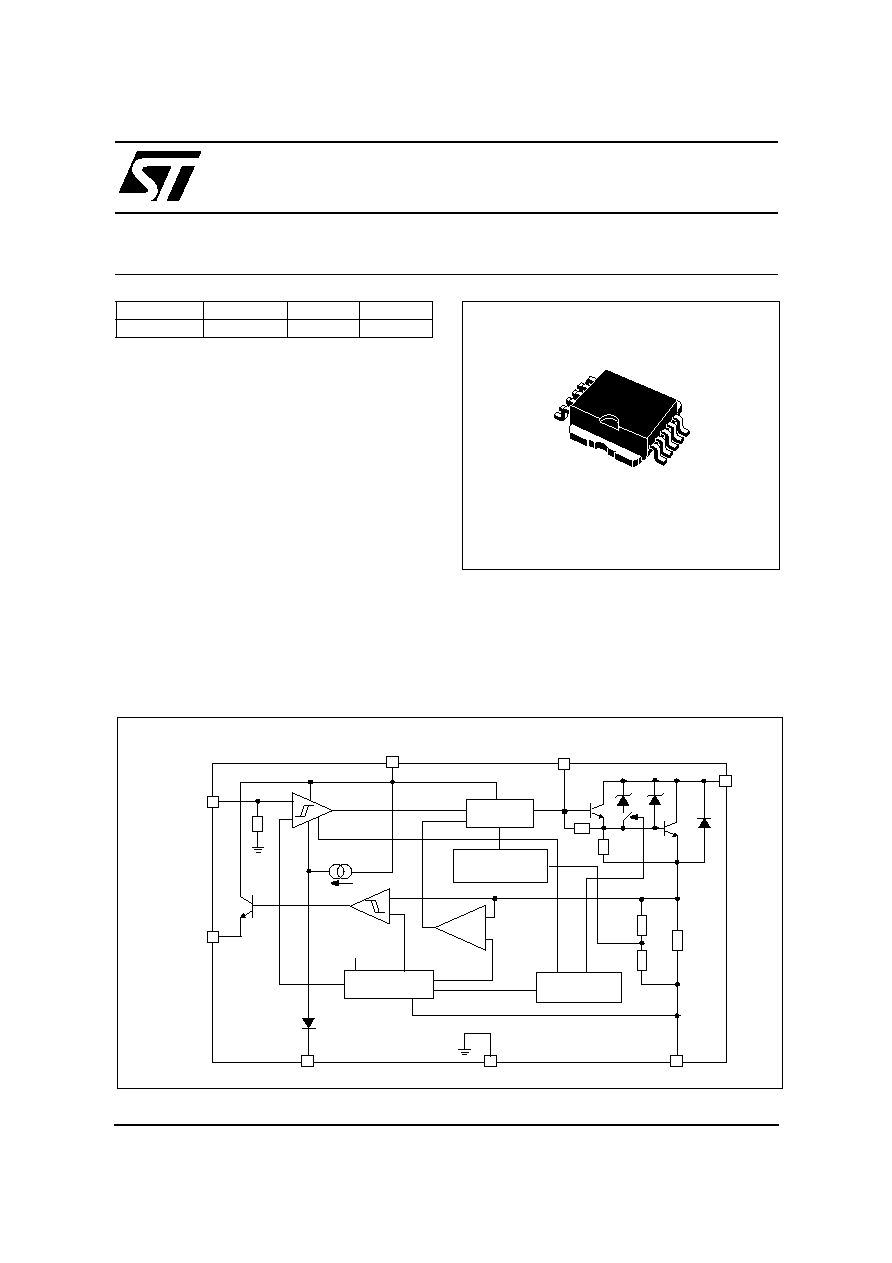
BLOCK DIAGRAM
PowerSO-10
TM
1
10
DRIVER
GND
REFERENCE
R
SENSE
V
CC
HV
C
V
IN
QUASI PROP.
BASE
CURRENT
-
THERMAL
PROTECTION
BD
E
DIAGNOSTIC
OUTPUT
V
CC
V
R
V
F1
V
LIM
V
TH
SN
LIMITER
LGND
2/9
VB326SP
ABSOLUTE MAXIMUM RATING
THERMAL DATA
PIN FUNCTION
(*) When grounded the Input is Enabled
CONNECTION DIAGRAM (TOP VIEW)
Symbol
Parameter
Value
Unit
HV
c
Collector voltage (Internally limited)
-0.3 to V
clamp
V
I
C
Collector current (Internally limited)
10
A
I
C(gnd)
DC current on Emitter Power
±
10.5
A
V
CC
Driving stage supply voltage
-0.3 to 7
V
I
s
Driving circuitry supply current
±
200
mA
I
s(gnd)
DC current on Ground pin
±
1
A
V
IN
Input voltage
-0.3 to V
CC
+ 0.3
V
I
IN
Maximum Input Current
100
mA
f
IN
Logic Input Frequency in Operative Mode
DC to 150
Hz
V
OUT(flag)
Output Voltage Primary Threshold Current Level
-0.3 to V
CC
+ 0.3
V
I
OUT(flag)
Flag Output Current
100
mA
P
max
Power Dissipation (T
c
=25∞C)
125
W
E
s/b
Self Clamped Energy during Output Power Clamping (See figure 2)
275
mJ
V
ESD
ESD voltage (HV
c
pin)
±
4
KV
V
ESD
ESD voltage (Enable pin)
+
1.5 ; -2
KV
V
ESD
ESD voltage (Other pins)
±
2
KV
I
BD
Input Darlington Base Current
150
mA
V
BD
Input Darlington Base Voltage
Internally limited
V
T
j
Operating Junction Temperature
-40 to 150
∞C
T
stg
Storage temperature Range
-55 to 150
∞C
V
E
Maximum Enable Voltage
-0.3 to 5.5
V
I
E
Maximum Enable Current
±
150
µ
A
Symbol
Parameter
Value
Unit
R
thj-case
Thermal resistance junction-case
(MAX)
1
∞C/W
R
thj-amb
Thermal resistance junction-ambient
(MAX)
51
∞C/W
No
Name
Function
1 - 5
LGND
Signal Ground
2 - 3 - 4
GND
Emitter Power Ground
6
E
Enable (*)
7
V
CC
Logic Supply Voltage
8
BD
Base Darlington
9
INPUT
Logic input channel (Internal Pull Down)
10
FLAG
Diagnostic Output Signal (Open Emitter)
TAB
HV
C
Primary Coil Output Driver (Open Collector)
1
2
3
4
5
6
7
8
9
10
TAB
LGND
GND
GND
GND
LGND
E
V
CC
BD
INPUT
FLAG
HV
C
Pin 1 and Pin 5 must be externally connected to Pins 2
˜
4.
3/9
VB326SP
ELECTRICAL CHARACTERISTICS
(5.3V < V
bat
< 24V; V
CC
=5V
±
10%; -40∫C < T
j
< 125∫C; R
coil
=580m
;
L
coil
=3.75mH unless otherwise specified; See note 1)
Note 1: parametric degratation are allowed with 5.3<V
b
<10V and V
b
>24V.
Note 2: the primary coil current value I
cl
must be measured 1ms after desaturation of the power stage.
Note 3: no internal Pull-down.
Note 4: if ENABLE pin is floating OUT=Off for every input status.
(*) Internally Limited
Symbol
Parameter
Test Conditions
Min
Typ
Max
Unit
V
cl
High
Voltage
Clamp
I
coil
=6.5A
320
360
420
V
V
lcl
Low Voltage Clamp
I
coil
=6.5A; T
j
=T
sd
30
40
50
V
V
ce(sat)
Power Stage Saturation
Voltage
I
C
=6A; V
IN
=4V
1.5
2
V
I
CC(stdby)
Stand-by Supply Current
IN=Off
11
mA
I
CC
DC Logic Current
V
b
=16V; I
C
=6.5A; f=100Hz; Load = Coil;
V
CC
=5.5V
40
mA
I
CC(peak)
Peak DC Logic Current
during On Phase
I
C
=6.5A
100
150
mA
V
CC
DC Logic Voltage
4.5
5.5
V
I
cl
Coil Current Limit
-40∫C < T
j
< 125∫C
(See note 2)
9
11
A
I
c(off)
Output Off State Current
IN=Off; V
HVC
=24V; V
CC
=5V; T
j
=25∫C
5
mA
T
Ic_ctr
Thermal Temperature
Output Current Control
OUT=On
150
(*)
∫C
V
INH
High Level Input Voltage
V
CC
=4.5V
4
V
CC
V
V
INL
Low Level Input Voltage
V
CC
=5.5V
-0.3
0.8
V
V
IN(hyst)
Input Threshold Hysteresis
0.4
V
I
INH
High Level Input Current
V
IN
=4V
100
µ
A
I
INL
Low Level Input Current
V
IN
=0.8V
0
30
µ
A
I
INpd
Input Active Pull Down
V
IN
=4V
10
100
µ
A
V
diagH
High Level Flag Output
Voltage
R
EXT
=22K
;
C
EXT
=1nF (See note 3)
V
CC
- 1
V
CC
V
V
diagL
Low Level Flag Output
Voltage
R
EXT
=22K
;
C
EXT
=1nF (See note 3)
0.5
V
I
diagTH
Coil Current Level Threshold T
j
=25∫C
6.15
6.5
6.85
A
I
diagTD
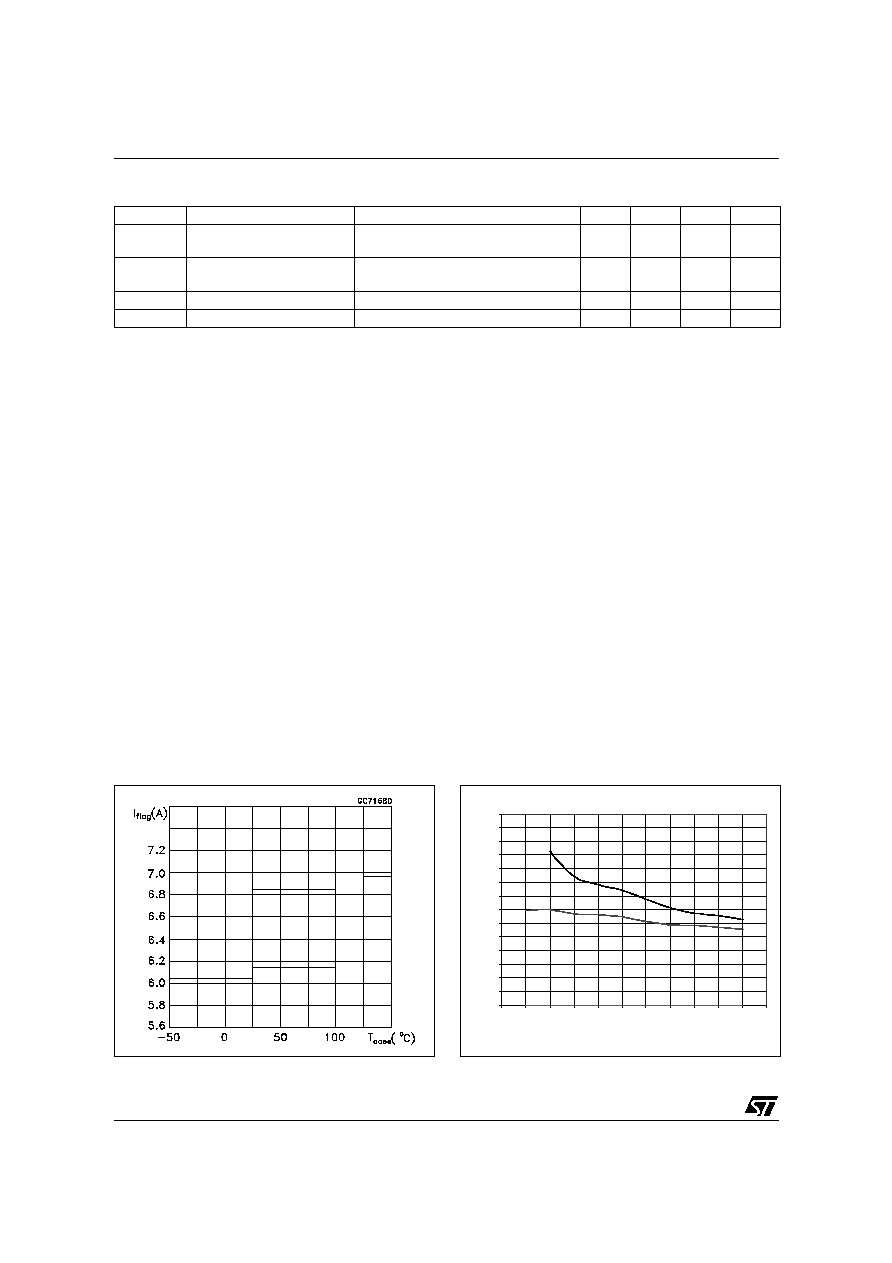
Coil Current Level Threshold
Drift
(See figure 1)
I
diag
High Level Flag Output
Current
I
C
> I
diagTH
; V
diag
=3V
0.5
mA
I
diag(leak)
Leakage Current on Flag
Output
V
IN
=Low; V
CC
=5.5V
10
µ
A
V
F
Antiparallel Diode Forward
Voltage
I
C
= -1A
2
V
E
s/b
Single Pulse Avalanche
Energy
L=6mH; I
C
= 8A (See figure 2)
180
mJ
t
ON
Turn-on time
R
c
=0.5
;
L
c
=3.75mH; T
j
=25∫C;
V
bat
=13V (See figure 6)
1
5
µ
s
t
OFF
Turn-off time
R
c
=0.5
;
L
c
=3.75mH; I
C
=6.5A; T
j
=25∫C;
V
bat
=13V (See figure 6)
15
25
µ
s
T
sd
Thermal shut-down
intervention
150
∫C
V
EH
High Level Enable Voltage
V
IN
=V
INH
; OUT=Off (See Note 4)
2
V
V
EL
Low Level Enable Voltage
V
OUT
free to follow V
IN
0.40
V
1
4/9
VB326SP
ELECTRICAL CHARACTERISTICS (continued)
Symbol
Parameter
Test Conditions
Min
Typ
Max
Unit
I
EH
High Level Sinked Enable
Current
V
E
=5V
500
µ
A
I
EL
Low Level Sinked Enable
Current
V
E
<0.4V
- 200
µ
A
V
BD(off)
Base Darlington Voltage Off
V
E
=V
EH
1
V
V
BD(on)
Base Darlington Voltage On
V
IN
=V
INH
; V
E
=V
EL
; I
C
=6.5A
1.8
V
1
PRINCIPLE OF OPERATION
The VB326SP is mainly intended as a high voltage
power switch device driven by a logic level input
and interfaces directly to a high energy electronic
ignition coil.
The input V
IN
of the VB326SP is fed from a low
power signal generated by an external controller
that determinesboth dwell time and ignition point.
During Vin high (
4V) the VB326SP increases
current in the coil to the desired, internally set
current level.
After reaching this level, the coil current remains
constant until the ignition point, that corresponds
to the transition of Vin from high to low (typ. 1.9V
threshold).
During the coil current switch-off, the primary
voltage HV
C
is clamped at an internally set value
V
cl
, typically 380V. The transition from saturation
to desaturation, coil current limiting phase, must
have the ability to accomodate an overvoltage.
A maximum overshoot of 20V is allowed.
FEEDBACK
When the collector current exceeds 6.5A, the
feedback signal is turned high and it remains so,
until the input voltage is turned-off.
OVERVOLTAGE
The VB326SP can withstand the following
transients of the battery line:
-100V/2msec(R
i
=10
)
+100V/0.2msec (R
i
=10
)
+50V/400msec (R
i
= 4.2
, with V
IN
= 3V)
Figure 1:
Flag current Vs. temperature
Figure 2:
Single pulse avalanche energy capability
0
50
100
150
200
250
300
350
400
450
500
550
600
650
700
0
10
20
30
40
50
60
70
80
90
100
110
L (mH)
E (
m
J
)
Tc=25∫
C
Tc=150∫
5/9
VB326SP
Figure 3: Self Clamped Inductive Switching
Current Vs. Time
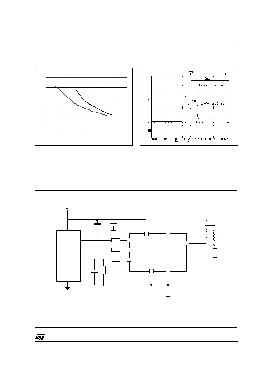
Figure 5: Typical application diagram
Figure 4: Low voltage clamp feature
µ
P
1nF
18K
V
CC
HV
C
GND
FLAG
V
bat
1
µ
F
100nF
E
LGND
V
IN
+5V
BD
1K
1K
1K
ENABLE pin can be alternatively connected to LGND
0
2
4
6
8
10
200
300
400
500
600
700
800
900
1000
Time in Clamp (µsec)
I
nduc
t
i
v
e
C
u
r
r
en
t
(
A
)
T=25∫
T=150∫