October 2000
1/7
Æ
VB921ZVFI
/
VB921ZVSP
HIGH VOLTAGE IGNITION COIL DRIVER
POWER I.C.
n
NO EXTERNAL COMPONENT REQUIRED
n
INTEGRATED HIGH VOLTAGE CLAMP
n
COIL CURRENT LIMIT INTERNALLY SE
T
n
HIGH RUGGEDNESS
DESCRIPTION
The VB921ZVFI, VB921ZVSP is a monolithic high
voltage integrated circuit made using the
STMicroelectronics VIPowerTM M1-2 technology,
which combines a vertical current flow power
trilinton with a coil current limiting circuit and a
collector voltage clamping. The device is
particularly suitable for application in high
performance electronic car ignition, where coil
current limitation and voltage clamping are
required.
TYPE
V
cl
I
cl
V
cg(sat)
VB921ZVFI
VB921ZVSP
340V
7.5A
2.5V
1
ISOWATT220
BLOCK DIAGRAM
PowerSO-10
TM
1
10
1
2
3
GND
ND8012
CONTROL
UNIT
R
SENSE
V
IN
HV
c
ORDER CODES:
ISOWATT220
POWERSO-10
TM
VB921ZVFI
VB921ZVSP

2/7
VB921ZVFI / VB921ZVSP
1
ABSOLUTE MAXIMUM RATING
THERMAL DATA
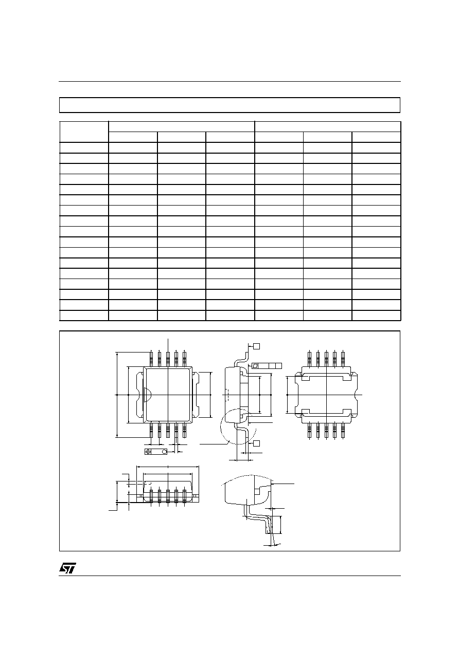
CONNECTION DIAGRAM (TOP VIEW)
Symbol
Parameter
Value
Unit
ISOWATT220
PowerSO-10
HV
c
Collector Voltage
Internally limited
V
I
C
Collector Current
Internally limited
A
V
IN
Maximum Input Voltage
8
V
I
IN
Input current
10
mA
P
tot
Total dissipation at T
C
=25
∞C
40
100
W
T
j
Junction operating temperature
- 40 to 150
∞C
T
stg
Storage temperature
- 40 to 150
∞C
Symbol
Parameter
Value
Unit
ISOWATT220
PowerSO-10
R
thj-case
Thermal resistance junction-case
(MAX)
3.12
1.25
∞C/W
R
thj-amb
Thermal resistance junction-ambient
(MAX)
62.5
62.5
∞C/W
ELECTRICAL CHARACTERISTICS
(V
CC
=12V; T
case
=25∫C unless otherwise specified)
(*) Coil data: primary resistance R
C
=0.4 ˜ 0.8
, primary inductance L
C
=6 ˜ 8mH
(**) Pulsed: pulse duration= 300
µ
s, duty cycle=1.5%
NOTE 1: I
cl
is also controlled in respect to the variation of V
IN
between 4.5 and 5.5V
Symbol
Parameter
Test Conditions
Min
Typ
Max
Unit
V
IN
Input Voltage
4.2
5.5
V
I
IN
Input Current
V
IN
=4.2V; I
C
=5A (See test circuit)
V
IN
=5V; I
C
=5A
5
10
mA
mA
I
cgo
Collector Cut-off Current
V
IN
=0V; HV
C
=250V
250
µ
A
V
cl
(*)
High voltage clamp
-40∞C<T
j
<125∞C
340
440
V
I
cl
(*)
Coil Current Limit
V
IN
=4.2V; -40∞C<T
j
<125∞C
V
IN
=5V; -40∞C<T
j
<125∞C
(See note 1)
6
6.5
7.5
A
A
V
cg(sat)
Power Stage Saturation
Voltage
I
C
=5A; I
IN
=10mA
2.5
V
V
f
(**)
Diode Forward Voltage
I
f
=10A
3.5
V
I
cl
Coil current variation in
respect to V
IN
=5V
V
IN
=4.5 ˜ 5.5V
200
mA
1
2
3
4
5
6
7
8
9
10
11
GND
GND
GND
GND
GND
V
IN
V
IN
V
IN
V
IN
V
IN
HV
C
3
2
1
V
IN
HV
C
GND

3/7
VB921ZVFI / VB921ZVSP
1
1
FIGURE 1: Delay-off time Vs Temperature
FIGURE 3: Saturation Voltage VS Collector Current
FIGURE 5: Coil Current Limit Vs Temperature
FIGURE 2: Input current Vs Temperature
FIGURE 4: Diode Forward Voltage VS Temperature
FIGURE 6: Clamping
Voltage VS Temperature
1