 | –≠–ª–µ–∫—Ç—Ä–æ–Ω–Ω—ã–π –∫–æ–º–ø–æ–Ω–µ–Ω—Ç: Y18 | –°–∫–∞—á–∞—Ç—å:  PDF PDF  ZIP ZIP |
Æ
1/6
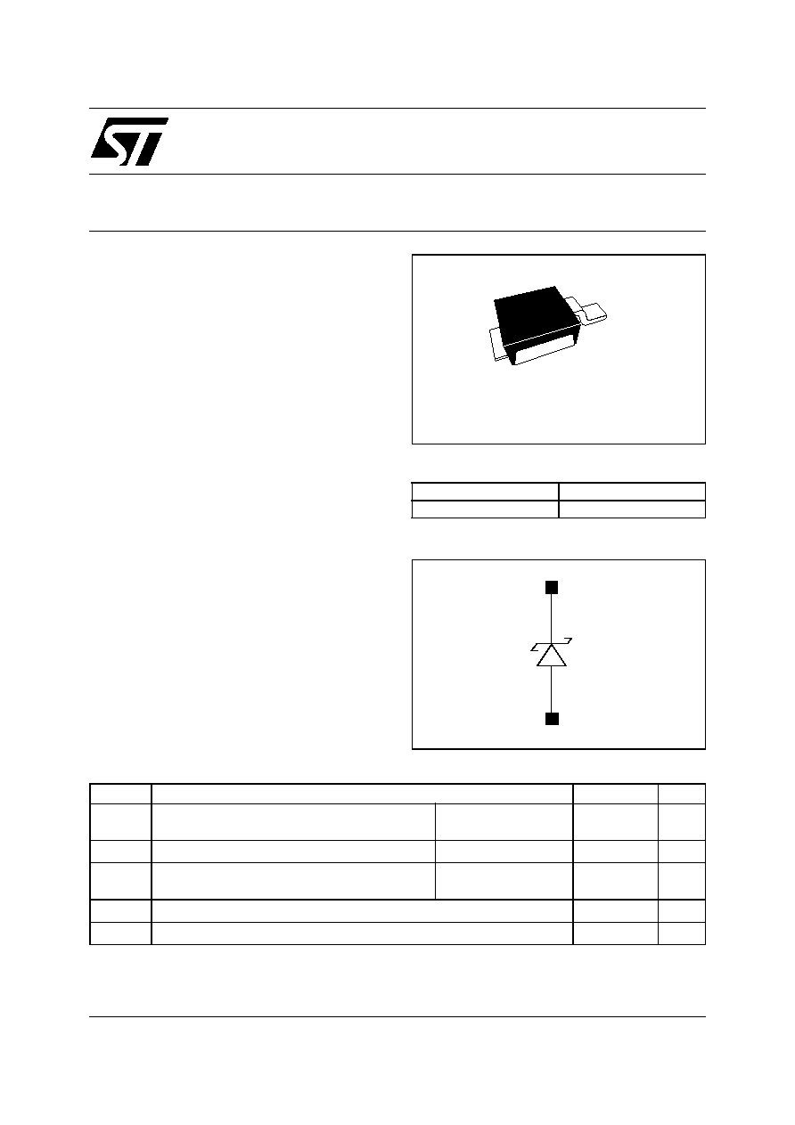
SMTY18AM
LOW FORWARD VOLTAGE TVS: TranskyTM
REV. 2
Table 2: Absolute Ratings (limiting values)
Note 1: 8/20µs pulse waveform
Symbol
Parameter
Value
Unit
V
PP
IEC 61000-4-2 standard
Air discharge
Contact discharge
15
8
kV
P
PP
Peak pulse power dissipation (see note 1)
Tj initial = Tamb
400
W
I
FSM
Non repetitive surge peak forward current
T
p
= 10 ms
Tj = initial = Tamb
25
A
T
stg
Storage temperature range
-65 to + 175
∞C
T
j
Maximum operating junction temperature
150
∞C
K
A
September 2004
FEATURES AND BENEFITS
High peak pulse power: 400W (8/20µs)
Stand-off voltage 16V
Low forward voltage: 0.48V @ 0.85A @ 25∞C
Low clamping factor V
CL
/V
BR
Fast response time
Very thin package (1.0mm overall component
height)
DESCRIPTION
The TranskyTM is designed specifically for portable
equipments and miniaturized electronics devices
subject to ESD transient overvoltages.
The TranskyTM combines the performance of a
TransilTM or TVS (Tansient Voltage Supressor)
and low forward voltage Schottky diode in a
monolithic structure.
COMPLIES WITH FOLLOWING STANDARDS
IEC 61000-4-2 Level 4:
15kV (Air discharge)
8kV
(Contact discharge)
MIL Standard 883E-Method 3015-7: class 3C
Human Body Model (HBM)
Table 1: Order Code
Part Number
Marking
SMTY18AM
Y18
K
A
STmite
(DO-216AA)

SMTY18AM
2/6
Table 3: Thermal Resistances
Table 4: Static Electrical Characteristics
(Tamb = 25∞C)
Note 2: Tamb = 85∞C
Note 3: 8/20µs pulse waveform
Note 4: Pulse test tp = 500µs, d< 2%
Symbol
Parameter
Value
Unit
R
th(j-a)
Junction to ambient on PCB with recommended pad layout
250
∞C/W
Symbol
Parameter
V
BR
Breakdown voltage
I
RM
Leakage current @ V
RM
V
RM
Stand-off voltage
V
CL
Clamping voltage
R
d
Dynamic impedance
I
PP
Peak pulse current
C
Capacitance
I
RM
max @ V
RM
Note 2
V
CL
max @ I
PP
Note 3
V
F
max @ 0.85A
Note 4
T max
C typ @ 0V
mA
V
V
A
V
10
-4
/∞C
pF
4
16
20
1
0.48
8.8
500
I
I
F
V
F
V
CL
V
BR
V
RM
I
PP
I
RM
V
I
R

SMTY18AM
3/6
Figure 1: Peak pulse power versus exponential
pulse duration
Figure 2: Relative variation of peak pulse
power versus initial junction temperature
Figure 3: Average power dissipation versus
ambient temperature
Figure 4: Variation of thermal impedance
junction to ambient versus pulse duration
(Epoxy FR4, e
cu
=35µm)
Figure 5: Thermal resistance junction to
ambient versus copper surface under tab
Figure 6: Reverse leakage current versus
junction temperature (typical values)
10
100
1000
0.01
0.10
1.00
10.00
t
p
(ms)
T
j
initial = 25∞C
P (W)
PP
0
10
20
30
40
50
60
70
80
90
100
110
0
25
50
75
100
125
150
175
T
j
(∞C)
%
0.0
0.1
0.2
0.3
0.4
0.5
0
25
50
75
100
125
150
T
amb
(∞C)
Printed circuit board FR4 (e
CU
=35µm)
µ
,
recommended pad layout
P(W)
0.1
1.0
10.0
100.0
1000.0
1.E-03
1.E-02
1.E-01
1.E+00
1.E+01
1.E+02
1.E+03
t
p
(s)
S
CU
=0.135cm≤≤
S
CU
=2cm≤≤
Zth(j-a)(∞C/W)
0
50
100
150
200
250
0.0
0.2
0.4
0.6
0.8
1.0
1.2
1.4
1.6
1.8
2.0
2.2
S
CU
(cm≤)
Rth(j-a)(∞C/W)
1.E+00
1.E+01
1.E+02
1.E+03
1.E+04
1.E+05
0
25
50
75
100
125
150
T
j
(∞C)
V
R
=V
RM
I (µA)
R

SMTY18AM
4/6
Figure 7: Clamping voltage versus peak pulse
current (typical values)
Figure 8: Junction capacitance versus reverse
voltage applied (typical values)
Figure 9: Forward voltage drop versus forward
current (typical values)
0.1
1.0
10.0
100.0
10
12
14
16
18
20
22
24
26
28
30
V
CL
(V)
8/20µs
10/1000µs
T
j
initial =25∞C
I (A)
PP
100
1000
1
10
100
V
R
(V)
F=1MHz
V
OSC
=30mV
RMS
T
j
=25∞C
C(pF)
0.01
0.10
1.00
10.00
0.0
0.1
0.2
0.3
0.4
0.5
0.6
0.7
0.8
0.9
1.0
V
F
(V)
T
j
=85∞C
T
j
=25∞C
I (A)
F

SMTY18AM
5/6
Figure 10: STmite Package Mechanical Data
Figure 11: Foot Print Dimensions (in millimeters)
C
L2
L
A1
R1
R
0∞ to 6∞
b
H
b2
D
L3
A
E
1.82
2.03
1.10
0.50
1.38
0.75
0.71
Table 5: Ordering Information
Ordering type
Marking
Package
Weight
Base qty
Delivery mode
SMTY18AM
Y18
STmite
15.5 mg
12000
Tape & reel
REF.
DIMENSIONS
Millimeters
Inches
Min.
Typ.
Max.
Min.
Typ.
Max.
A
0.85
1.00
1.15 0.033 0.039 0.045
A1
-0.05
0.05 -0.002
0.002
b
0.40
0.65 0.016
0.025
b2
0.70
1.00 0.027
0.039
c
0.10
0.25 0.004
0.010
D
1.75
1.90
2.05 0.069 0.007 0.081
E
1.75
1.90
2.05 0.069 0.007 0.081
H
3.60
3.75
3.90 0.142 0.148 0.154
L
0.50
0.63
0.80 0.019 0.025 0.031
L2
1.20
1.35
1.50 0.047 0.053 0.059
L3
0.50
ref
0.019
ref
R
0.07
0.003
R1
0.07
0.003
Table 6: Revision History
Date
Revision
Description of Changes
09-Jul-2004
1
First issue
13-Sep-2004
2
STmite package dimensions reference A1 change: from
blank (min) to -0.05mm and from 0.10 (max) to 0.05mm.