 | –≠–ª–µ–∫—Ç—Ä–æ–Ω–Ω—ã–π –∫–æ–º–ø–æ–Ω–µ–Ω—Ç: S42WD42 | –°–∫–∞—á–∞—Ç—å:  PDF PDF  ZIP ZIP |

SUMMIT MICROELECTRONICS, Inc. ∑ 300 Orchard City Drive, Suite 131 ∑ Campbell, CA 95008 ∑ Telephone 408-378-6461 ∑ Fax 408-378-6586 ∑ www.summitmicro.com
1
© SUMMIT MICROELECTRONICS, Inc. 2000
2025 6.0 4/17/00
Characteristics subject to change without notice
FEATURES
∑
Precision Dual Voltage Monitor
≠ V
CC
Supply Monitor
- Dual reset outputs for complex
microcontroller systems
- Integrated memory write lockout function
- No external components required
∑
Second Voltage Monitor Output
≠ Separate V
LOW
output
≠ Generates interrupt to MCU
≠ Generates RESET for dual supply systems
- Guaranteed output assertion to V
CC
- 1V
∑
Watchdog Timer (S42WD42, S42WD61)
≠ 1.6s
∑
Memory Internally Organized 2 x8
∑
Extended Programmable Functions
Available on SMS24
Dual Voltage Supervisory Circuit
With Watchdog Timer(S42WD61) (S42WD42)
S4242/S42WD42/S4261/S42WD61
∑
High Reliability
≠ Endurance: 100,000 erase/write cycles
≠ Data retention: 100 years
OVERVIEW
The S42xxx are a precision power supervisory circuit. It
automatically monitors the device's V
CC
level and will
generate a reset output on two complementary open drain
outputs. In addition to the V
CC
monitoring, the S42xxx also
provides a second voltage comparator input. This input
has an independent open drain output that can be wire-
OR'ed with the RESET I/O or it can be used as a system
interrupt.
The S42xxx also has an integrated 4k/16k-bit nonvolatile
memory. The memory conforms to the industry standard
two-wire serial interface. In addition to the reset circuitry,
the S42WD42/S42WD61 also has a watchdog timer.
BLOCK DIAGRAM
PROGRAMMABLE
WATCHDOG
TIMER
+
≠
GND
VCC
8
4
RESET#
2
VTRIP
RESET
CONTROL
RESET
7
1.26V
SCL
6
SDA
5
2025 T BD 2.0
WRITE
CONTROL
NONVOLATILE
MEMORY
ARRAY
PROGRAMMABLE
RESET PULSE
GENERATOR
+
≠
VLOW#
UV
OV
VSENSE 3
1
(S42WD42,
S42WD61)
2
S4242/S42WD42/S4261/S42WD61
2025 6.0 4/17/00
ABSOLUTE MAXIMUM RATINGS
Temperature Under Bias
............................................................................................................................... -40∞C to +85∞C
Storage Temperature
..................................................................................................................................... -65∞C to +125∞C
Soldering Temperature (less than 10 seconds) ................................................................................................................... 300∞C
Supply Voltage
............................................................................................................................................................. 0 to 6.5V
Voltage on Any Pin
....................................................................................................................................... -0.3V to V
CC
+0.3V
ESD Voltage (JEDEC method) .......................................................................................................................................... 2,000V
NOTE: These are STRESS ratings only. Appropriate conditions for operating these devices are given elsewhere in this specification. Stresses
beyond those listed here may permanently damage the part. Prolonged exposure to maximum ratings may affect device reliability.
2.7V to 4.5V
4.5V to 5.5V
Symbol
Parameter
Conditions
Min
Max
Min
Max
Units
f
SCL
SCL Clock Frequency
0
100
400
KHz
t
LOW
Clock Low Period
4.7
1.3
µs
t
HIGH
Clock High Period
4.0
0.6
µs
t
BUF
Bus Free Time
Before New Transmission
4.7
1.3
µs
t
SU:STA
Start Condition Setup Time
4.7
0.6
µs
t
HD:STA
Start Condition Hold Time
4.0
0.6
µs
t
SU:STO
Stop Condition Setup Time
4.7
0.6
µs
t
AA
Clock to Output
SCL Low to SDA Data Out Valid
0.3
3.5
0.2
0.9
µs
t
DH
Data Out Hold Time
SCL Low to SDA Data Out Change
0.3
0.2
µs
t
R
SCL and SDA Rise Time
1000
300
ns
t
F
SCL and SDA Fall Time
300
300
ns
t
SU:DAT
Data In Setup Time
250
100
ns
t
HD:DAT
Data In Hold Time
0
0
ns
T
I
Noise Spike Width
Noise Suppression Time Constant
100
100
ns
@ SCL, SDA Inputs
t
WR
Write Cycle Time
10
10
ms
AC ELECTRICAL CHARACTERISTICS
(over recommended operating conditions unless otherwise specified)
2025 PGM T3.0
2025 PGM T2.0
DC ELECTRICAL CHARACTERISTICS (over recommended operating conditions unless otherwise specified)
Symbol
Parameter
Conditions
Min
Max
Units
SCL = CMOS Levels @ 100KHz
V
CC
=5.5V
3
mA
I
CC
Supply Current (CMOS)
SDA = Open
All other inputs = GND or V
CC
V
CC
=3.3V
2
mA
I
SB
Standby Current (CMOS)
SCL = SDA = V
CC
V
CC
=5.5V
50
µA
All other inputs = GND
I
LI
Input Leakage
V
IN
= 0 To V
CC
10
µA
I
LO
Output Leakage
V
OUT
= 0 To V
CC
10
µA
V
IL
Input Low Voltage
SCL, SDA, RESET# (pin 2)
0.3xV
CC
V
V
IH
Input High Voltage
SCL, SDA, RESET (pin7)
0.7xV
CC
V
V
OL
Output Low Voltage
I
OL
= 3mA SDA
0.4
V
V
CC
=3.3V
25
µA
Temperature
Min
Max
Commercial
0∞C
+70∞C
Industrial
-40∞C
+85∞C
RECOMMENDED OPERATING CONDITIONS
2025 PGM T1.0

S4242/S42WD42/S4261/S42WD61
3
2025 6.0 4/17/00
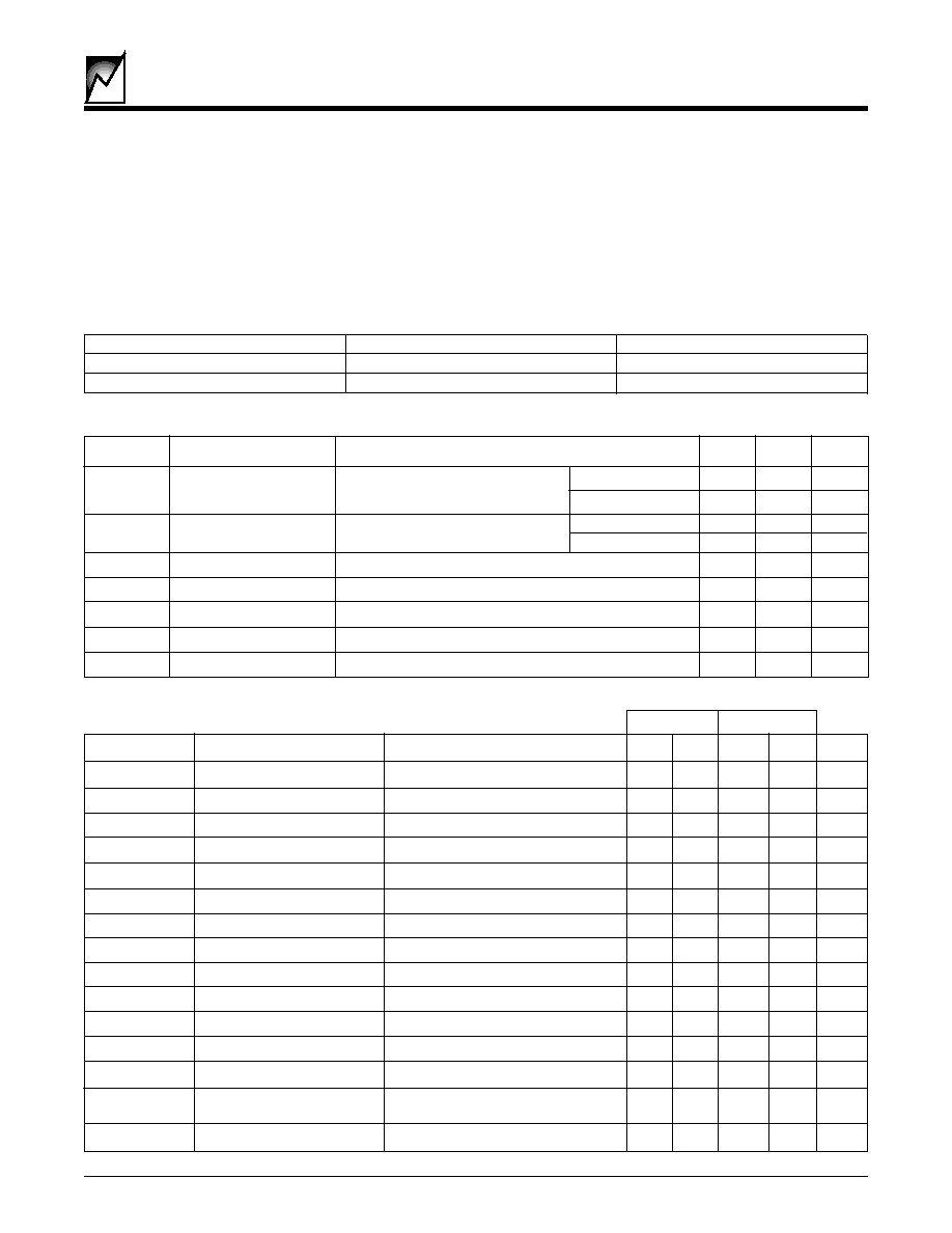
FIGURE 2. START AND STOP CONDITIONS
FIGURE 1. BUS TIMING
CAPACITANCE
T
A
= 25∞C, f = 100KHz
Symbol
Parameter
Max
Units
CIN
Input Capacitance
5
pF
C
OUT
Output Capacitance
8
pF
2025 PGM T4.0
tF
tR
tLOW
tHIGH
tHD:SDA
tSU:SDA
tBUF
tDH
tHD:DAT
tSU:DAT
tSU:STO
SCL
SDA In
SDA Out
tAA
2025 Fig01 1.0
2025 Fig02 1.0
SCL
SDA In
START
Condition
STOP
Condition

4
S4242/S42WD42/S4261/S42WD61
2025 6.0 4/17/00
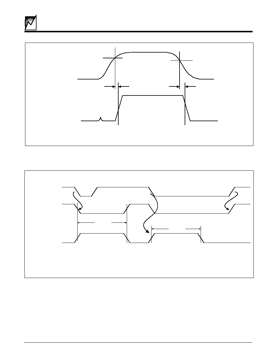
FIGURE 3. RESET OUTPUT TIMING
RESET CIRCUIT AC and DC ELECTRICAL CHARACTERISTICS
TA=-40∞C to +85∞C
Symbol
Parameter
Part no.
Min.
Typ.
Max.
Unit
Suffix
V
TRIP
Reset Trip Point
A (or) Blank
4.250
4.375
4.5
V
B
4.50
4.625
4.75
V
2.7
2.7
2.9
3.10
V
t
PURST
Reset Timeout
200
ms
t
RPD
V
TRIP
to RESET Output Delay
5
µs
V
RVALID
RESET Output Valid to V
CC
min. Guarantee
1
V
t
GLITCH
Glitch Reject Pulse Width note 1
30
ns
V
OLRS
RESET Output Low Voltage I
OL
= 1mA
0.4
V
V
OHRS
RESET High Voltage Output I
OH
= 800µA
V
CC
-.75
V
V
ULH
V
SENSE
Under-voltage threshold low to high
1.20
1.25
1.30
V
V
UHL
V
SENSE
Under-voltage threshold high to low
1.20
1.25
1.30
V
V
OLH
V
SENSE
Over-voltage threshold low to high
1.20
1.25
1.30
V
V
OHL
V
SENSE
Over-voltage threshold high to low
1.20
1.25
1.30
V
t
VD1
Delay to V
LOW
Active
5
µs
t
VD2
Delay to V
LOW
Released
5
µs
t
WDTO
Watchdog timeout Period (S42WD61)
1600
ms
(S42WD42)
2025 PGM T5.2
VCC
VRVALID
VTRIP
tPURST
RESET
2025 T fig03 2.0
tGLITCH
tRPD
tPURST
tRPD
RESET#
S4242/S42WD42/S4261/S42WD61
5
2025 6.0 4/17/00
FIGURE 4. V
SENSE
UNDER-VOLTAGE FUNCTION
FIGURE 5. RESET AS AN INPUT
2025 T fig05 2.0
t
PURST
t
PURST
RESET (out)
RESET# (in)
RESET# (out)
2025 T fig04 2.0
V
ULH
V
UHL
t
VD2
t
VD1
V
SENSE
(Under-voltage detect)
V
LOW
#