
©
SUMMIT MICROELECTRONICS, Inc. 2001 ∑ 300 Orchard City Drive, Suite 131 ∑ Campbell, CA 95008 ∑ Telephone 408-378-6461 ∑ Fax 408-378-6586 ∑ www.summitmicro.com
1
S93462/S93463
Characteristics subject to change without notice
Precision Supply-Voltage Monitor and Reset Controller
SUMMIT
MICROELECTRONICS, Inc.
2021 4.2 1/23/01
FEATURES
∑
Precision Monitor & RESET Controller
-- RESET and RESET Outputs
-- Guaranteed RESET Assertion to V
CC
= 1V
-- 150ms Reset Pulse Width
-- Internal 1.26V Reference with ±1% Accuracy
-- ZERO External Components Required
∑
Memory
-- 1K-bit Microwire Memory
-- S93462
≠ Internally Ties ORG Low
≠ 100% Compatible With all 8-bit
Implementations
≠ Sixteen Byte Page Write Capability
-- S93463
≠ Internally Ties ORG High
≠ 100% Compatible With all 16-bit
Implementations
≠ Eight Word Page Write Capability
OVERVIEW
The S93462 and S93463 are precision power supervi-
sory circuits providing both active high and active low
reset outputs.
Both devices have 1k-bits of E
2
PROM memory that is
accessible via the industry standard microwire bus. The
S93462 is configured with an internal ORG pin tied low
providing a 8-bit byte organization and the S93463 is
configured with an internal ORG pin tied high providing
a 16-bit word organization. Both the S93462 and
S93463 have page write capability. The devices are
designed for a minimum 100,000 program/erase cycles
and have data retention in excess of 100 years.
BLOCK DIAGRAM
+
≠
GND
VCC
8
5
RESET#
6
VTRIP
RESET
PULSE
GENERATOR
5kHz
OSCILLATOR
RESET
CONTROL
MODE
DECODE
ADDRESS
DECODER
WRITE
CONTROL
DATA I/O
E2PROM
MEMORY
ARRAY
RESET
7
1.26V
SK
2
DI
3
WATCHDOG
TIMER
CS
1
2021 T BD 2.0
DO
4

2
S93462/S93463
2021 4.2 1/23/01
Summit Microelectronics, Inc.
PIN FUNCTIONS
Pin Name
Function
CS
Chip Select
SK
Clock Input
DI
Serial Data Input
DO
Serial Data Output
V
CC
+2.7 to 6.0V Power Supply
GND
Ground
RESET/RESET#
RESET I/O
PIN CONFIGURATION
DEVICE OPERATION
APPLICATIONS
The S93462/463 is ideal for applications requiring low
voltage and low power consumption. This device pro-
vides microcontroller RESET control and can be manu-
ally resettable.
RESET CONTROLLER DESCRIPTION
The S93462/463 provides a precision reset controller
that ensures correct system operation during brownout
and power-up/-down conditions. It is configured with two
open drain reset outputs; pin 7 is an active high output
and pin 6 is an active low output.
During power-up, the reset outputs remain active until
V
CC
reaches the V
TRIP
threshold. The outputs will con-
tinue to be driven for approximately 150ms after reach-
ing V
TRIP
. The reset outputs will be valid so long as V
CC
is
1.0V. During power-down, the reset outputs will
begin driving active when V
CC
falls below V
TRIP
.
The reset pins are I/Os; therefore, the S93462/463 can
act as a signal conditioning circuit for an externally
applied reset. The inputs are edge triggered; that is, the
RESET input will initiate a reset time-out after detecting
a low to high transition and the RESET# input will initiate
a reset time-out after detecting a high to low transition.
Refer to the applications Information section for more
details on device operation as a debounce/reset ex-
tender circuit.
It should be noted the reset outputs are open drain.
When used as outputs driving a circuit they need to be
either tied high (
RESET#
) or tied to ground (RESET)
through the use of pull-up or pull-down resistors. Refer
to the applications aid section for help in determining the
value of resistor to be used. Internally these pins are
weakly pulled up (
RESET#
) and pulled down (RESET):
therefore, if the signals are not being used the pins may
be left unconnected.
GENERAL OPERATION
The S93462/463 is a 1024-bit nonvolatile memory
intended for use with industry standard microproces-
sors. The S93463 is organized as X16, seven 9-bit
instructions control the reading, writing and erase
operations of the device. The S93462 is organized as
X8, seven 10-bit instructions control the reading, writing
and erase operations of the device. The device operates
on a single 3V or 5V supply and will generate on chip, the
high voltage required during any write operation.
Instructions, addresses, and write data are clocked into
the DI pin on the rising edge of the clock (SK). The DO
pin is normally in a high impedance state except when
reading data from the device, or when checking the
ready/busy status after a write operation.
The ready/busy status can be determined after the start
of a write operation by selecting the device (CS high) and
polling the DO pin; DO low indicates that the write
operation is not completed, while DO high indicates that
the device is ready for the next instruction. See the
Applications Aid section for detailed use of the ready
busy status.
CS
SK
DI
DO
VCC
RESET
RESET#
GND
1
2
3
4
8
7
6
5
8-Pin PDIP
or 8-Pin SOIC
2021 T PCon 2.0

3
S93462/S93463
2021 4.2 1/23/01
Summit Microelectronics, Inc.
The format for all instructions is: one start bit; two op
code bits and either six (x16) or seven (x8) address or
instruction bits.
Read
Upon receiving a READ command and an address
(clocked into the DI pin), the DO pin of the S93462/463
will come out of the high impedance state and, will first
output an initial dummy zero bit, then begin shifting out
the data addressed (MSB first). The output data bits
will toggle on the rising edge of the SK clock and
are stable after the specified time delay
(t
PD0
or t
PD1
).
Write
After receiving a WRITE command, address and the
data, the CS (Chip Select) pin must be deselected for a
minimum of 250ns (t
CSMIN
). The falling edge of CS will
start automatic erase and write cycle to the memory
location specified in the instruction. The ready/busy
status of the S93462/463 can be determined by select-
ing the device and polling the DO pin.
Erase
Upon receiving an ERASE command and address, the
CS (Chip Select) pin must be deselected for a minimum
of 250ns (t
CSMIN
). The falling edge of CS will start the
auto erase cycle of the selected memory location. The
ready/busy status of the S93462/463 can be deter-
mined by selecting the device and polling the DO pin.
Once cleared, the content of a cleared location returns
to a logical "1" state.
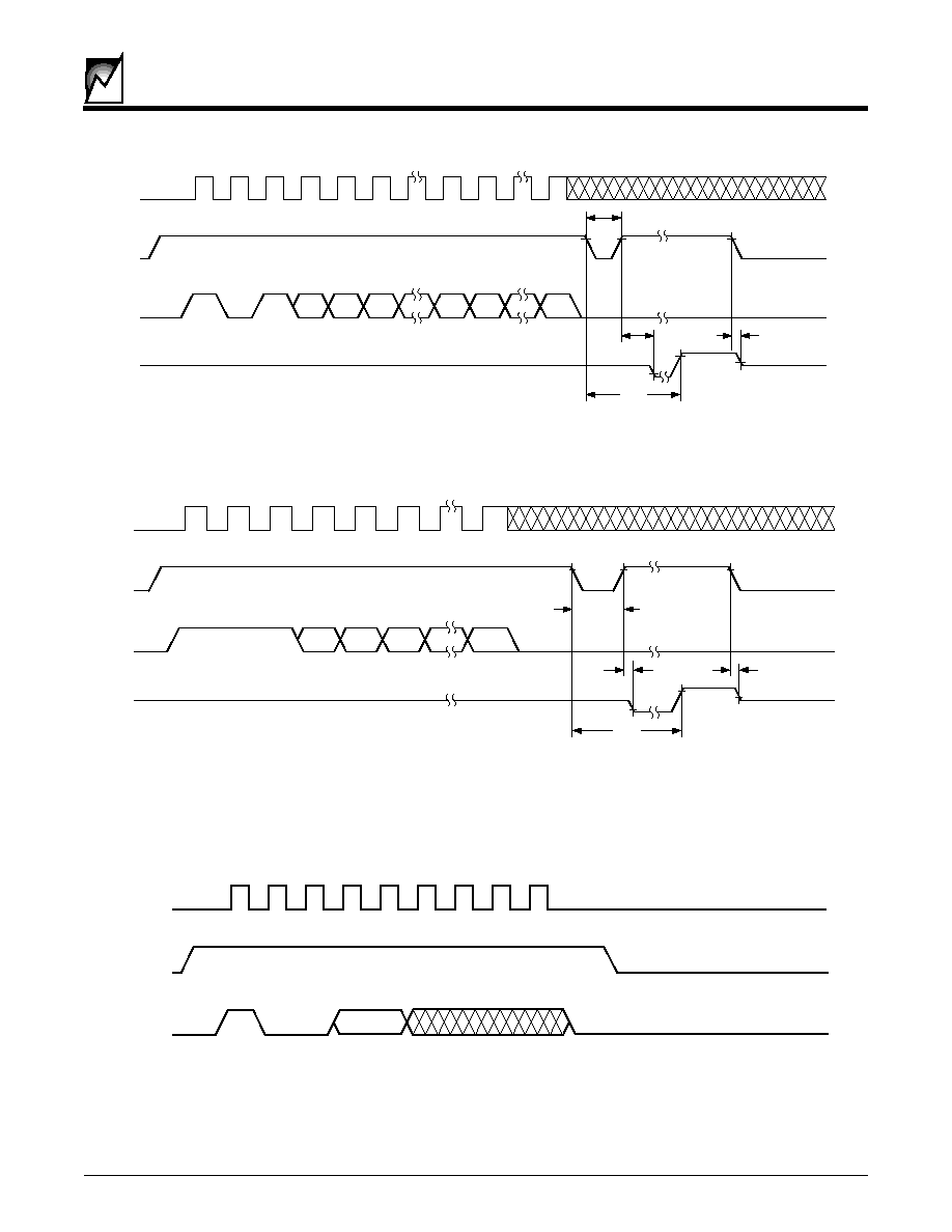
Figure 1. Sychronous Data Timing
Figure 2. Read Instruction Timing
SK
2021 ILL 3 1.0
DI
CS
DO
t DIS
t
PD0,
t
PD1
tCSMIN
tCSS
tDIS
tDIH
tSKHI
t CSH
VALID
VALID
DATA V ALID
t SKLOW
SK
2021 ILL4 1.0
CS
DI
DO
tCS
STANDBY
tHZ
HIGH-Z
HIGH-Z
1
1
0
AN AN≠1
A0
0
DN DN≠1
D1
D0
tPD0

4
S93462/S93463
2021 4.2 1/23/01
Summit Microelectronics, Inc.
Erase/Write Enable and Disable
The S93462/463 powers up in the write disable state.
Any writing after power-up or after an EWDS (write
disable) instruction must first be preceded by the EWEN
(write enable) instruction. Once the write instruction is
enabled, it will remain enabled until power to the device
is removed, or the EWDS instruction is sent. The EWDS
instruction can be used to disable all S93462/463 write
and clear instructions, and will prevent any accidental
writing or clearing of the device. Data can be read
normally from the device regardless of the write enable/
disable status.
Erase All
Upon receiving an ERAL command, the CS (Chip
Select) pin must be deselected for a minimum of 250ns
(t
CSMIN
). The falling edge of CS will start the self clocking
clear cycle of all memory locations in the device. The
clocking of the SK pin is not necessary after the device
has entered the self clocking mode. The ready/busy
status of the S93462/463 can be determined by select-
ing the device and polling the DO pin. Once cleared, the
contents of all memory bits will be in a logical "1" state.
Write All
Upon receiving a WRAL command and data, the CS
(Chip Select) pin must be deselected for a minimum of
250ns (t
CSMIN
). The falling edge of CS will start the self
clocking data write to all memory locations in the device.
The clocking of the SK pin is not necessary after the
device has entered the self clocking mode. The ready/
busy status of the S93462/463 can be determined by
selecting the device and polling the DO pin. It is not
necessary for all memory locations to be cleared before
the WRAL command is executed.
Page Write
93462 - Assume WEN has been issued. The host will
then take CS high, and begin clocking in the start bit,
write command and 7-bit address immediately fol-
lowed by the first byte of data to be written. The host
can then continue clocking in 8-bit bytes of data with
each byte to be written to the next higher address.
Internally the address pointer is incremented after
receiving each group of eight clocks; however, once
the address counter reaches xxx 1111 it will roll over
to xxx 0000 with the next clock. After the last bit is
clocked in no internal write operation will occur until CS
is brought low.
93463 - Assume WEN has been issued. The host will
then take CS high, and begin clocking in the start bit,
write command and 6-bit address immediately
followed by the first 16-bit word of data to be written.
The host can then continue clocking in 16-bit words of
data with each word to be written to the next higher
address. Internally the address pointer is incremented
after receiving each group of sixteen clocks; however,
once the address counter reaches xxx x111 it will roll
over to xx x000 with the next clock. After the last bit is
clocked in no internal write operation will occur until CS
is brought low.
Continuous Read
This begins just like a standard read with the host
issuing a read instruction and clocking out the data
byte [word]. If the host then keeps CS high and
continues generating clocks on SK, the S93462/463
will output data from the next higher address location.
The S93462/463 will continue incrementing the ad-
dress and outputting data so long as CS stays high. If
the highest address is reached, the address counter
will roll over to address 0000. CS going low will reset
the instruction register and any subsequent read must
be initiated in the normal manner of issuing the com-
mand and address.
5
S93462/S93463
2021 4.2 1/23/01
Summit Microelectronics, Inc.
SK
2021 ILL 5 1.0
CS
DI
DO
tCS
STANDBY
HIGH-Z
HIGH-Z
1
0
1
AN
AN-1
A0
DN
D0
BUSY
READY
STATUS
VERIFY
tSV
tHZ
tEW
SK
2021 ILL6 1.0
CS
DI
DO
STANDBY
HIGH-Z
HIGH-Z
1
AN
AN-1
BUSY
READY
STATUS VERIFY
tSV
tHZ
tEW
tCS
1
1
A0
Figure 3. Write Instruction Timing
Figure 4. Erase Instruction Timing
Figure 5. EWEN/EWDS Instruction Timing
SK
2021 Fig05
CS
DI
STANDBY
1
0
0
*
* ENABLE = 11
DISABLE = 00