SUMMIT MICROELECTRONICS, Inc. ∑ 300 Orchard City Drive, Suite 131 ∑ Campbell, CA 95008 ∑ Telephone 408-378-6461 ∑ Fax 408-378-6586 ∑ www.summitmicro.com
1
Characteristics subject to change without notice
© SUMMIT MICROELECTRONICS, Inc. 1999
2037 8.0 8/8/00
SUMMIT
MICROELECTRONICS, Inc.
SMH4042
FEATURES
∑
Full Voltage Control for Hot Swap Applications
CompactPCI High Availability Compatible
-
On-board 15V High Side Driver Generation
Allows use of Low On-resistance N-Channel FETS
-
Undervoltage Lockout
-
Electronic Circuit Breakers
-
Card Insertion Detection
-
Host VCC Detection
-
Card Voltage Sequencing
∑
Flexible Reset Control
-
Low Voltage Resets
-
Host Reset Filtering
-
Soft Reset
∑
Adjustable Power-on Slew Rate
∑
Supports Mixed Voltage Cards
∑
Integrated 4K Bit 2-Wire E
2
PROM Memory
-
Data DownloadTM Mode [Simplifies
Downloading of Configuration Memory into
Interface ASIC or MCU]
APPLICATIONS
∑
CompactPCI Hot Swap Control
∑
VME Live Insertion Control
Hot SwapTM Controller
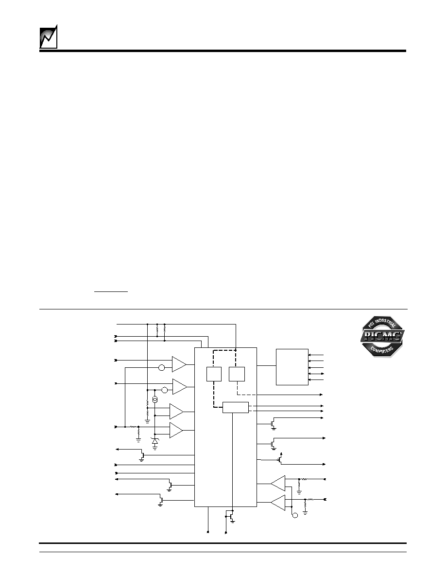
DESCRIPTION
The SMH4042 is a fully integrated hot swap controller that
provides complete power control for add-in cards ranging
in use for basic hot swap systems to high availability
systems. It detects proper insertion of the card and
senses valid supply voltage levels at the backplane.
Utilizing external low on-resistance N-channel
MOSFETs, card power is ramped by two high-side driver
outputs that are slew-rate limited at 250V/s.
The SMH4042 continuously monitors the host supplies,
the add-in card supplies and the add-in card current. If the
SMH4042 detects the current is higher than the pro-
grammed value it will shut down the MOSFETs and issue
a fault status back to the host.
The on board E
2
PROM can be used as configuration
memory for the individual card or as general purpose
memory. The proprietary DataDownload mode provides
a more direct interface to the E
2
PROM, simplifying access
by the add-in card's controller or ASIC.
FUNCTIONAL BLOCK DIAGRAM
ASSOCIATE
MEMBER
VGATE3
VGATE5
ISLEW
BD_SEL1#
SGNL_VLD#
HEALTHY#
VCC5
HST_3V_MON
VSEL
PCI_RST#
CARD_3V_MON
CARD_5V_MON
+
-
LOCAL_PCI_RST#
LOCAL_PCI_RST
DRVREN#
+
-
+
-
EEPROM
Memory
Array
A2
SCL
SDA
A1
A0
BD_SEL2#
+
-
+
-
+
-
PWR_EN
FAULT#
1Vref
1.25V
Slew Rate
Control
Charge
Pump
Ref
Voltage
Control
Circuitry
50mV
_+
_+
50mV
CBI_3
CBI_5
2037 ILL2.2
2
SMH4042
2037 8.0 8/8/00
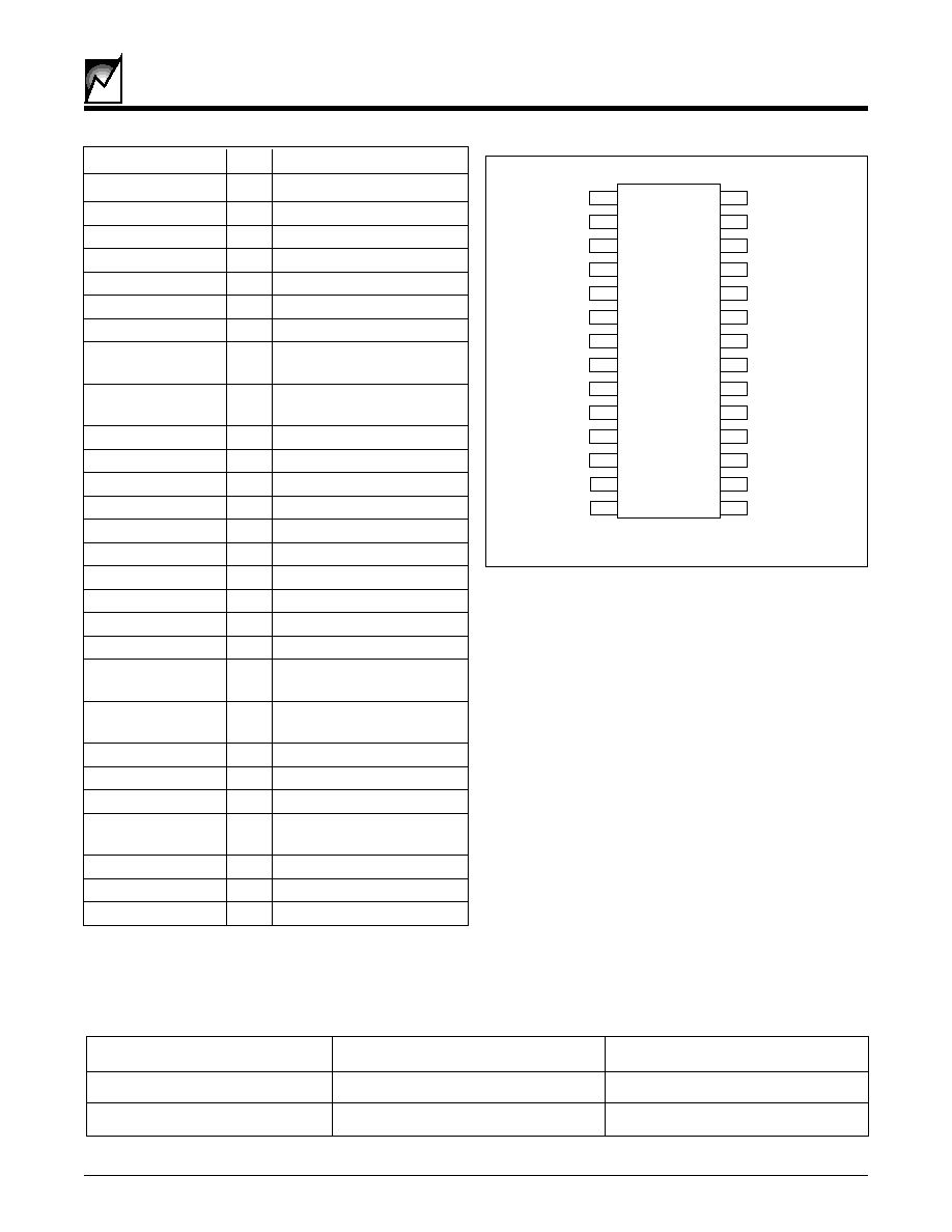
PIN CONFIGURATIONS SOIC and SSOP
RECOMMENDED OPERATING CONDITIONS
Condition
Min
Max
Temperature
-40∞C
+85∞C
V
CC
2.7V
5.5V
2037 PGM T2.0
Symbol
Pin
Description
CBI_5
1
Circuit Breaker Input (5V)
DRVREN#
2
High Side Driver Enable
ISLEW
3
Slew Rate Control
FAULT#
4
Fault Output Active Low
1Vref
5
1Volt Reference Output
VSEL
6
Voltage Select Input
PWR_EN
7
Power On Enable Input
A0
8
Memory Address 0
(NC or Gnd)
LOCAL_PCI_RST#
9
Back End Reset Output
(Active Low)
A1
10
Memory Address 1
A2
11
Memory Address 2
BD_SEL2#
12
Board Select 2
BD_SEL1#
13
Board Select 1
GND
14
Ground
HEALTHY#
15
Backend Power On
SGNL_VLD#
16
Signals Valid Output
PCI_RST#
17
Host reset input
SDA
18
Serial Data I/O
SCL
19
Serial Clock Input
LOCAL_PCI_RST
20
Back End Reset
Output
(Active High)
CARD_3V_MON
21
Card-side 3 Volt
Monitor Input
VGATE3
22
High Side Drive Output
HST_3V_MON
23
Host 3V Monitor Input
CBI_3
24
Circuit Breaker Input (3V)
CARD_5V_MON
25
Card-side 5 Volt
Monitor Input
NC
26
No Connect
VGATE5
27
High Side Drive Output
V
CC
28
Supply Voltage
2037 PGM T1.2
1
2
3
4
5
6
7
8
9
10
11
12
24
23
22
21
20
19
18
17
16
15
27
28
VCC
VGATE5
CARD_5V_MON
HST_3V_MON
VGATE3
CARD_3V_MON
SDA
SGNL_VLD#
HEALTHY#
GND
BD_SEL2#
CBI_5
DRVREN#
ISLEW
VSEL
PWR_EN
A0
LOCAL_PCI_RST#
A1
A2
PCI_RST#
1Vref
13
14
25
26
CBI_3
BD_SEL1#
LOCAL_PCI_RST
FAULT#
SCL
NC
2037 ILL1.2
3
2037 8.0 8/8/00
SMH4042
*COMMENT
Stresses listed under Absolute Maximum Ratings
may cause permanent damage to the device. These
are stress ratings only, and functional operation of
the device at these or any other conditions outside
those listed in the operational sections of this speci-
fication is not implied. Exposure to any absolute
maximum rating for extended periods may affect
device performance and reliability.
ABSOLUTE MAXIMUM RATINGS*
Temperature Under Bias
-55∞C to +125∞C
Storage Temperature
-65∞C to +150∞C
Voltage on :
HST_3V_MON, CARD_3V_MON
7V
V
CC
, CARD_5V_MON
SGNL_VLD#, HEALTHY# &
7V
LOCAL_PCI_RESET#
VGATE3, VGATE5, DRVREN#
16V
RESET
V
CC
+.7V
All Others
V
CC
+.7V
Output Short Circuit Current
100mA
Lead Solder Temperature (10 secs)
300∞C
Symbol
Parameter
Part no.
Min.
Typ.
Max.
Units
Suffix
V
CC
Operating Voltage
See Note 1
1
V
I
CC1
Power Supply Current
Operating
500
µA
I
CC2
Power Supply Current
Writing
3
mA
V
TRIP
V
TRIP
Threshold Levels
V
CC
5
A
4.250
4.375
4.50
V
V
CC
5
B
4.50
4.625
4.75
V
HST_3V_MON
G
2.57
2.65
2.72
V
HST_3V_MON
H
2.72
2.8
2.87
V
HST_3V_MON
K
2.87
2.95
3.0
V
HST_3V_MON
L
3.0
3.1
3.17
V
CARD_5V_MON
M
V
CC
5 V
TRIP
V
+50mV
CARD_5V_MON
N
V
CC
5 V
TRIP
V
-50mV
CARD_3V_MON
M
HST_3V_MON
V
+50mV
CARD_3V_MON
N
HST_3V_MON
V
-50mV
V
TRHST
Trip Point Hysteresis
7
mV
I
LI
Input Leakage Current
2
µA
I
LO
Output Leakage Current
10
µA
V
IL
Input Low Voltage
-0.1
0.8
V
V
IH
Input High Voltage
2
V
CC
+1V
V
V
OL
Output Low Voltage, V
CC
= 5.0V, I
OL
= 2.1mA
0.4
V
V
OH
Output High Voltage, V
CC
= 5.0V, I
OH
= -400µA
2.4
V
V
OLRS
LOCAL_PCI_RESET# Output Low Voltage, I
OL
= 3.2mA
0.4
V
V
OHRS
RESET Output High, I
OH
= -800µA
V
CC
-.75V
V
V
OHVG
VGATE3, VGATE5 Output Voltage, I
OH
= 20µA
13
14
15
V
V
REF
Reference Output Voltage, No Load
0.95
1
1.05
V
V
CB
Circuit Breaker Trip Voltage, V
CB
(V
CC
-CBI_5) or
40
50
60
mV
V
CB
=(HST_3V_MON-CBI_3)
DC ELECTRICAL CHARACTERISTICS T
A
= -40∞C to +85∞C
2037 PGM T3.4
Notes:
1. The SMH4042 will drive the reset outputs and voltage control signals to valid levels throughout the operating range of 1V to 5.5V.
The balance of the logic will not be guaranteed operational unless V
CC
is greater than 2.7V.
2. Refer to the ordering information table for all valid combinations of options.
4
SMH4042
2037 8.0 8/8/00
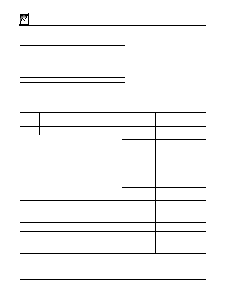
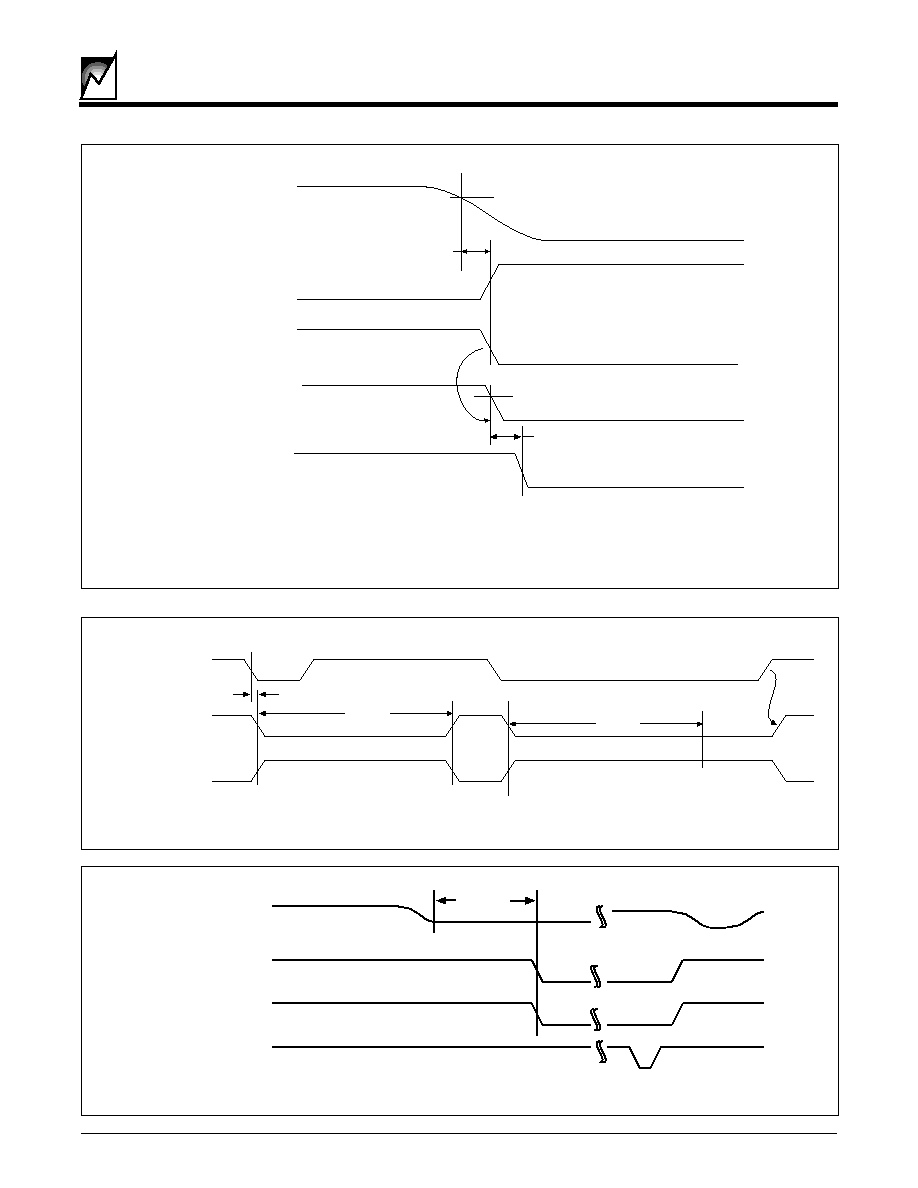
Card Insertion Timing Diagram
V
TRIP
V
RVALID
VCC
&
HST_3V_MON
LOCAL_PCI_RST#
RESET
BD_SEL1#
+
BD_SEL2#
VGATE5 & VGATE3
DRVREN#
CARD_5V_MON
&
CARD_3V_MON
HEALTHY#
SGNL_VLD#
V
TRIP
t
PURST
t
SLEW
t
HSE
V
OHVG
2037 ILL3.0
Symbol
Parameter
Notes
Min.
Typ.
Max.
Units
t
VTPD
V
TRIP
to Power Down Delay
Host Voltage Input
1
5
µs
t
VTR
V
TRIP
to RESET Output Delay
Card Voltage Input
1
5
µs
t
PRLPR
PCI_RST# to LOCAL_PCI_RST#
.1
1
µs
V
RVALID
RESET Output Valid
1
V
T
SLEW
Slew Rate
250
V/Sec
T
HSE
BD-SEL# to Power-on Delay
BD_SEL# Noise filter
100
150
200
ms
t
PURST
Reset Timeout
100
150
200
ms
t
GLTICH
Glitch Reject Pulse Width
40
ns
t
OCF
Over-current to FAULT#
1
µs
t
OCVG
Over-current to VGATE Off
1
µs
t
CBTC
Circuit Breaker Time Constant
Powering-on
4
µs
Operating
16
µs
SEQUENCER AC OPERATING CHARACTERISTICS (Over Recommended Operating Conditions)
2037 PGM T4.1
5
2037 8.0 8/8/00
SMH4042
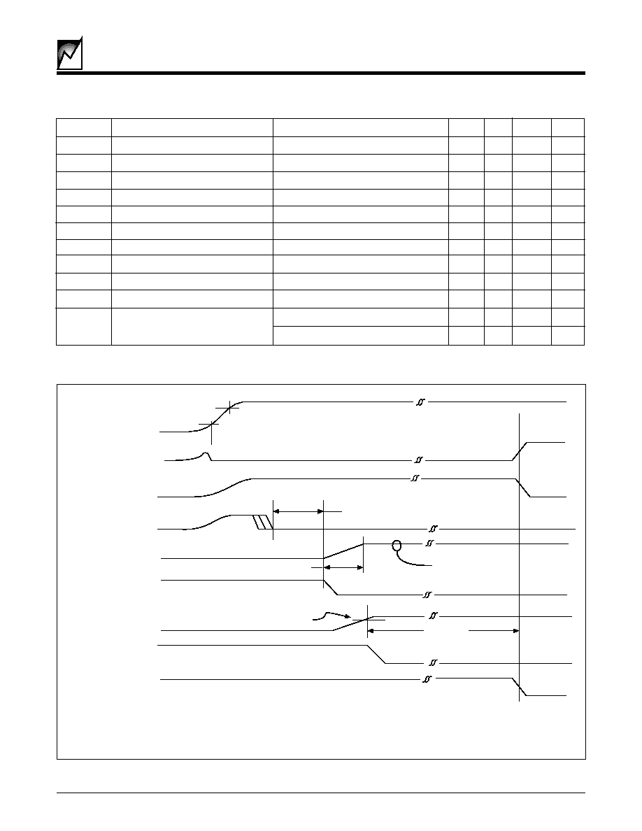
Loss of Voltage Timing Sequence
Circuit Breaker Timing Diagram
Host Initiated Reset Timing Diagram
VCC
or
HST_3V_MON
VGATE5
&
VGATE3
LOCAL_PCI_RST#
&
HEALTHY#
SGNL_VLD#
&
DRVREN#
t
VTPD
CARD_5V_MON
or
CARD_3V_MON
V
TRIP
V
TRIP
t
VTR
2037 ILL4.0
t
PRLPR
PCI_RST#
LOCAL_PCI_RST#
RESET
t
PURST
t
PURST
2037 ILL5.0
t
CBTC
CBI_5 or CBI_3
FAULT#
VGATE5 & VGATE3
PCI_RST#
2037 ILL6.0