Programmable Adaptive Laser Power Controller with Dual Lookup Tables
Preliminary Information
1
(See Last Page)
� SUMMIT Microelectronics, Inc. 2004 � 1717 Fox Drive � San Jose CA 95131-2312 � Phone 408 436-9890 � Fax 408 436-9897 � www.summitmicro.com
2066 6.3 1/22/04
1
SML2120
�
FEATURES AND APPLICATIONS
Features:
� Integrated Automatic Power Control (APC) circuit
� 100 mA bias current sink capability
� Dual low-current outputs (up to 2.5 mA) based on two
independent 256x8 Lookup Table values
� Bias current and/or temperature monitoring capability
� Dual high/low alert registers
� Advanced lookup algorithm eliminates unnecessary
output changes
� Flexible voltage operation;
0 to 5V, 0 to 3.3V, or -5.2V to +3.3V
� I
2
C 2-wire serial bus interface for programming
configuration, control values, monitoring, and
operational status - 100KHz and 400KHz
� Small 5X5 28-Pin QFN Package
Applications:
� Laser power management for Telecom/Datacom
motherboards
� Direct modulation and electro-absorptive modulation
applications
�
INTRODUCTION
The SML2120 is an advanced, programmable laser diode
power controller ideal for optical networking applications.
The integrated automatic power control (APC) circuit adapts
to variations in the laser's power output as detected by a
photo diode.
The SML2120 drives two low current outputs derived from
values stored in independent 256x8 Lookup Tables. The low
current outputs are suitable for controlling the MODSET
input of typical laser driver IC's. The input stimulus for each
Lookup Table can be configured as the laser temperature,
the bias current, or an external signal. Characteristics of the
laser's performance over time and temperature are stored
in the lookup tables, allowing the outputs to adapt to system
conditions and optimize overall performance.
Programming of configuration and control values by the
user are simplified with the I
2
C interface adapter
(SMX3200) and Windows Programming software available
from Summit Microelectronics.
�
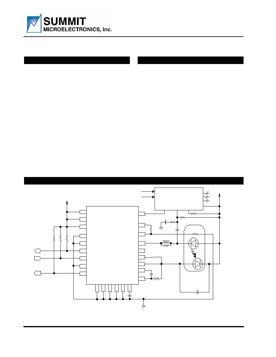
SIMPLIFIED APPLICATION DRAWING
Figure 1. Typical SML2120 Connections to a Laser Driver and Laser Diode
SML2120
V
DD
(+3.3V)
ILU1
THERMISTOR
14
11
20
18
BIAS
MPD
16
17
C1
C2
13
10
21
9
VS
S
15
24
25
VDD
VHI
+3.3V
8V
L
O
W
EN
A
#
1
2
3
4
5
A1
A2
SDA
SCL
6
7
AM#
ALERT#
A
d
d
r
ess = 0
DATA�
DATA+
MODSET
BIASMAX
APCSET
CAPC
V
DD
OUT�
OUT+
No Co
nne
c
t
s
Typical
Laser Driver
Typical Laser
Diode with
Photo Diode
and Thermistor
ILU0
C
INT
R
INT
12
VBRIDGE
NTC
LD
MPD
VDD
VS
S
VS
S
EXT_TEMP
23
22
VA
P
C
Note: This is an applications example only. Some pins, components and values are not shown.

Functional Description
SML2120
2
2066 6.3 1/22/04
Summit Microelectronics
�\
FUNCTIONAL DESCRIPTION
The SML2120 is an adaptive power controller for laser
diodes. The device contains an active feedback loop used
to calibrate and control the mean and modulation power of
high-speed high-power laser diodes.
Inherent manufacturing tolerances introduce variations of
performance in laser diodes. These variations, combined
with parametric changes over the laser's extreme operating
temperature range and laser aging, require an efficient
compensation solution. The SML2120, together with a
minimum number of external components, is designed to
compensate for these variations using a digital control loop
and dual programmable nonvolatile calibration lookup
tables.
Figure 2 shows the output light power of a typical laser
diode versus its operating current. Depicted in the graph are
laser diode characteristics at two different temperatures. At
the first temperature (T
Cold
), the laser requires an average
bias current of I
BIAS1
. The modulation current required to
switch the laser between its ON and OFF states is labeled
I
MOD1
.
The ratio of light power of its ON state divided by the light
power of its OFF state is referred to as the extinction ratio.
Ideally the laser requires a constant extinction ratio over its
entire operating temperature range, as the receiver module
is calibrated to this level. Operating the laser driver at a
higher extinction ratio indicates that power is being wasted,
whereas operating at a lower extinction ratio indicates that
data may possibly be lost.
The required bias current increases to I
BIAS2
when the laser
is operated at a second temperature (T
Hot
). The laser
requires a modulation of I
MOD2
to maintain a constant
extinction ratio as in the T
Cold
curve. The SML2120, with its
dual lookup table architecture (Figure 3), is capable of
providing variable output currents based on a function of
either the bias current or the external temperature, and
thereby enables the system designer to optimize the
extinction ratio of the laser driver module.
The SML2120 eliminates the need for any manual
calibration of the laser control circuit. All calibration values
are programmed through the I
2
C industry-standard 2-wire
communication interface whose protocol and functions can
be controlled by automated test equipment (ATE).
Figure 2. Laser Current Increase Caused by Temperature Increase, Constant Light Power Out
SML2120
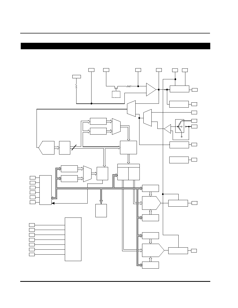
Functional Block Diagram
Summit Microelectronics
2066 6.3 1/22/04
3
�
FUNCTIONAL BLOCK DIAGRAM
Figure 3. SML2120 Block Diagram
10-BIT ADC
Comparison
Logic
Alarm
Logic
Address Decode
256 x 8
E
2
PROM
Lookup
Table
256 x 8
E
2
PROM
Lookup
Table
CH1 Previous
Conversion
CH2 Previous
Conversion
CH1 High/Low
Limits
CH2 High/Low
Limits
8-BIT DAC
High Range
DAC
Low Range
DAC
+
-
Quick
Start
18
MPD
17
16
1
28
BIASMON
23
11
EXT_TEMP
THERMISTOR
8-BIT DAC
High Range
DAC
Low Range
DAC
2
3
4
5
7
I
2
C
2-Wire
Serial
Interface
A1
SCL
A2
SDA
ALERT#
13
ILU1
27
TEMPMON
26
POWERMON
Power
Distribution
8
9
10
VSS
VSS
VLOW
VSS
15
21
VDD
VHI
VDD
25
24
C1
C2
ENA#
6
AM#
Bias to Voltage
Converter
MPD to Voltage
Converter
14
20
BIAS
Current Generator
256 x 8
E
2
PROM
General
Purpose
Scale
&
Offset
8
ILU0
19
VBURST
Current Generator
Current Generator
Temp to Voltage
Converter
22
VAPC
0.75V
Internal
Reference
12
VBRIDGE
Bridge
Circuit
VSS
+
-
+
-
Package and Pin descriptions
SML2120
4
2066 6.3 1/22/04
Summit Microelectronics
�
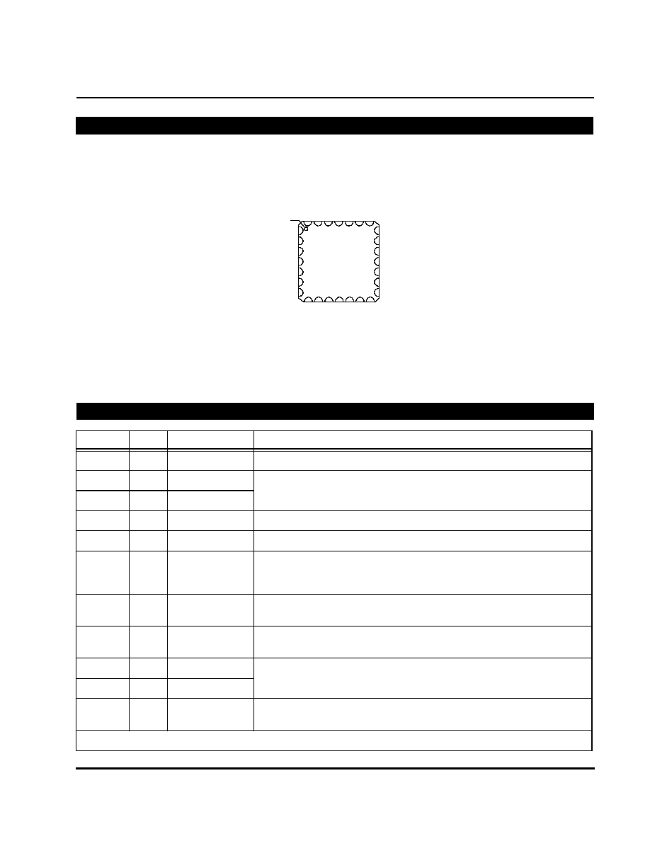
PACKAGE AND PIN DESCRIPTIONS
Figure 4. 28-Pin QFN Package Pinout (top view)
PIN DESCRIPTIONS
PIN DESCRIPTIONS
Pin 1
ENA#
A1
A2
SDA
SCL
AM#
ALERT#
VSS
BIAS
VBURST
MPD
C1
C2
VDD
VL
OW
VS
S
VS
S
THERMI
ST
OR
V
B
RIDGE
IL
U0
IL
U1
BI
ASMO
N
TEMPMO
N
PO
WERMON
VHI
VDD
EX
T_
TM
P
V
APC
Pin Number Pin Type
Pin Name
Description
1
I
ENA#
*
Active low input enables the BIAS, ILU0 and ILU1 output currents.
2
I
A1*
The address pins are connected to either the VHI or VLOW pins to provide a
mechanism for assigning a unique I
2
C bus address to the SML2120.
3
I
A2
*
4
I/O
SDA
*
Bi-directional I
2
C serial data pin
5
I
SCL
*
I
2
C serial clock input
6
I
AM#
*
AM# is an active low input, when asserted the SML2120 is placed in the Auto-
Monitor mode. AM# must be high for programming the Configuration registers
and the Lookup Tables, ILU0 and ILU1 and the general purpose E
2
PROM.
7
O
ALERT#
*
Active low, open-drain output indicates when one of the monitored inputs
exceeds its user-programmable high or low alert levels.
8
PWR
VLOW
In dual-rail supply voltage systems, VLOW is tied to the system logic low
potential. It is a logic low reference for all pins marked with an asterisk (*).
9
PWR
VSS
VSS must be tied to the lowest system voltage potential.
10
PWR
VSS
11
I
THERMISTOR
Connect a thermistor to this pin to provide an alternative source of temperature
sensing (see VBRIDGE description).
* See VLOW and VHI pin descriptions.
PACKAGE AND PIN DESCRIPTIONS
PIN DESCRIPTIONS

SML2120
Pin Descriptions
Summit Microelectronics
2066 6.3 1/22/04
5
12
O
VBRIDGE
Connection to an external Full-Bridge Sensor when used with the Thermistor pin.
Two of the full-bridge resistors are internal. See the Bridge Circuit Diagram in
Figure 1 and 3. Voltage level is 0.2V with respect to VSS.
13
I/O
ILU0
Current output resulting from Lookup Table 0. User-programmable to either sink
(to VSS) or source (to VDD) up to 2.5mA.
14
I/O
ILU1
Current output resulting from Lookup Table 1. User-programmable to either sink
(to VSS) or source (to VDD) up to 2.5mA.
15
PWR
VDD
VDD is the positive rail for most internal functions.
16
I
C2
Place a capacitor (C
INT
) between C1 and C2 to increase the time constant for the
APC integrator.
17
I
C1
18
I
MPD
Monitor Photo Diode anode input. Connect a resistor between MPD and C1 to
work in conjunction with C
INT
to establish the integrator time constant.
19
I
VBURST
In burst mode, this input supplies a ballast current that allows the SML2120 to
quickly restart when ENA# is asserted.
20
I
BIAS
Supplies the main laser current as controlled by the APC circuit; capable of
sinking up to 100mA to VSS.
21
PWR
VSS
VSS must be tied to the lowest system voltage potential.
22
I/O
VAPC
APC Override pin.
23
I
EXT_TEMP
This input can be configured to sense either a voltage or current generated from
an external temperature monitoring device.
24
PWR
VDD
VDD is the positive rail for most internal functions.
25
PWR
VHI
In dual-voltage rail systems, VHI is tied to the system logic high potential. It is the
logic high reference for all pins marked with an asterisk (*).
26
O
POWERMON
*
Analog output voltage indicating the state of the Monitor Photo Diode (MPD)
input.
27
O
TEMPMON
*
Analog output voltage proportional to the temperature as sensed by the
EXT_TEMP or THERMISTOR input.
28
O
BIASMON
*
Analog output voltage proportional to BIAS current.
* See VLOW and VHI pin descriptions.
Pin Number Pin Type
Pin Name
Description