SMM150
Preliminary Information
1
(See Last Page)
© SUMMIT Microelectronics, Inc. 2005 ∑
1717 Fox Drive ∑ San Jose CA 95131 ∑ Phone 408 436-9890 ∑ FAX 408 436-9897
www.summitmicro.com
2075 2.6 05/13/05
1
FEATURES
∑ Capable of margining supplies with trim inputs
using either positive or negative trim pin control
∑ Wide Margin range from 0.3V to VDD using
internal reference
∑ 10-bit ADC readout of supply voltage over I
2
C bus
∑ Margining Controlled Via:
I
2
C Command
Input Pins (M
UP
, M
DN
)
∑ Two programmable general purpose sensor inputs
(COMP1/2) ≠ UV/OV with FAULT Output
∑ Programmable glitch filter (COMP1/2)
∑ Programmable internal VREF, 0.5V or 1.25V
∑ Operates from 2.7V to 5.5V supply
∑ General Purpose 256-Byte EEPROM with Write
Protect
∑ I
2
C 2-wire serial bus for programming
configuration and monitoring status
∑ 28 lead QFN
∑ 20 ball Ultra CSP
TM
(Chip-Scale) package
Applications
∑ In-system test and control of Point-of-Load (POL)
Power Supplies for Multi-voltage Processors,
DSPs and ASICs
∑ Routers, Servers, Storage Area Networks
INTRODUCTION
The SMM150 is a highly accurate power supply
voltage supervisor and environmental monitor with
provisions for voltage margining of the monitored supply.
The part includes an internal voltage reference to
accurately monitor and margin the supply to within ±1%.
The SMM150 has the capability to margin over a wide
range from 0.3V to VDD using the internal reference and
can read the value of the supply over the I
2
C bus using
an on-chip 10-bit ADC. The monitor and margin levels
are set using the I
2
C serial bus. The SMM150 initiates
margining via the I
2
C bus or by using the M
UP
or M
DN
inputs. Once the pre-programmed margin target voltage
is reached, the SMM150 holds the converter at this
voltage until receiving an I
2
C command or de-asserting
the margin input pin. When the SMM150 is not
margining, the TRIM output pin is held in a high
impedance state allowing the converter to operate at its
nominal set point. Two general purpose input pins are
provided for sensing under or overvoltage conditions. A
programmable glitch filter associated with these inputs
allows the user to ignore spurious noise signals. A
FAULT# pin is asserted once either input set point is
exceeded.
Using the I
2
C interface, a host system can communicate
with the SMM150 status register and utilize 256-bytes of
nonvolatile memory.
SIMPLIFIED APPLICATIONS DRAWING
VM
TRIM
TRIM
VOUT+
SEN+
DC-DC Converter
VDD
WP
A0
A1
A2
COMP1
COMP2
SCL
SDA
FAULT#
CAPM
MUP
MDN
I
2
C
Interface
Margin
Commands
V1
2.7V-5.5V
SMM150
READY
GND
VDD_CAP
Status
Outputs
Figure 1 ≠ Applications using the SMM150 Controller to control the Voltage Margining of a DC/DC Converter.
Note: This is an applications example only. Some components and values are not shown.
Single-Channel Supply Voltage Marginer/Monitor

SMM150
Preliminary Information
Summit Microelectronics, Inc
2075 2.6 05/13/05
2
GENERAL DESCRIPTION
The SMM150 is capable of margining the DC output
voltage of LDOs or DC/DC converters that use a
trim/adjust pin. The Margin function is programmable
over a standard 2-wire I
2
C serial data interface and is
used to set the margin low/high DC output voltages.
In margining mode the user communicates with the
SMM150 via the I
2
C serial data bus to select the
desired values for margining. This allows the part to
margin the supplies up or down to these set values
either through asserting the MUP and MDN pins or by
writing to the margin register directly. The margin high
and margin low voltage settings can range from 0.3V
to VDD around the converter's nominal output voltage
setting depending on the specified margin range of the
DC-DC converter and/or system components, usually
±
10%.
When the SMM150 receives the command to margin,
the TRIM output will begin adjusting the supply to the
selected margin voltage. This is accomplished by
incrementing (or decrementing) an internal counter
based on the digital comparison between the voltage
margin target value and that read by the ADC from the
VM input. This operation is repeated until the 2 values
are equal, after which the SMM150 holds the TRIM
output pin at the voltage required to maintain the
margin setting. An I
2
C command or de-assertion of the
MUP/MDN pin will return the TRIM output pin to a high
impedance state thus allowing the converter to return
to its nominal operating voltage.
The SMM150 has two additional input pins and one
additional output pin. The input pins, COMP1 and
COMP2, are high impedance inputs, each connected
to a comparator and compared against the internal
reference (VREF, 0.5V or 1.25V). Each comparator
can be independently programmed to monitor for UV
or OV. When either of the COMP1 or COMP2 inputs
are in fault the open-drain FAULT# output will be
pulled low. A configuration option exists to disable the
FAULT# output during margining.
Programming of the SMM150 is performed over the
industry standard I
2
C 2-wire serial data interface. A
status register is available to read the state of the part
and a Write Protect (WP) pin is available to prevent
writing to the configuration registers and EE memory.

SMM150
Preliminary Information
Summit Microelectronics, Inc
2075 2.6 05/13/05
3
VM
Control
Logic
TRIM
10Bit
ADC
Digital
Comparator
8-bit DAC
I
2
C
Interface
Clock
Up/Dn
Halt
Margin
Target
OV/UV
OV/UV
Output
Control
VDD
WP
A0
A1
A2
COMP1
COMP2
SCL
SDA
FAULT#
EE
Configuration
Registers
& Memory
GND
Glitch
Filter
V
REF
SW1
SW2
MUX
CAPM
MUP
MDN
READY
VREF =
1.25V or 0.5V
50k
50k
VDD_CAP
VREF
Figure 2 ≠ SMM150 Controller Internal Block Diagram.
PACKAGE AND PIN CONFIGURATION
1
28
21
20
19
18
17
16
15
22
23
24
25
26
27
2
3
4
5
6
7
14
13
SMM150
Pin 1
SCL
A2
NC
A1
READY
A0
GND
WP
NC
CA
P
_
M
FAU
LT#
NC
CO
M
P
2
VM
VDD
TRIM
COMP1
NC
NC
NC
NC
SDA
NC
NC MDN MUP V
D
D_
CA
P
NC
12
11
10
9
8
GND
or
NC
INTERNAL BLOCK DIAGRAM
28 Pad QFN
Top View
A1
A2
A4
A3
B1
B2
B4
B3
C1
C2
C4
C3
D1
D2
D4
D3
E1
E2
E4
E3
SCL
MDN VDD_CAP VDD
A2
SDA
TRIM
COMP1
A1
READY
MUP
NC
A0
WP
FAULT#
NC
GND
CAP_M COMP2
VM
Pin 1
20 Ball Ultra CSP
TM
Bottom View
SMM150
Preliminary Information
Summit Microelectronics, Inc
2075 2.6 05/13/05
4
PIN DESCRIPTIONS
QFN
Pad
Number
Ultra
CSP
TM
Ball
Number
Pin
Type
Pin Name
Pin Description
28
B2
I/O
SDA
I
2
C Bi-directional data line
1
A1
I
SCL
I
2
C clock input.
2
B1
I
A2
4
C1
I
A1
6
D1
I
A0
The address pins are biased either to VDD, GND or left floating. This
allows for a total of 21 distinct device addresses. When
communicating with the SMM150 over the 2-wire bus these pins
provide a mechanism for assigning a unique bus address.
8
D2
I
WP
Programmable Write Protect active high/low input. When asserted,
writes to the configuration registers and general purpose EE are not
allowed. The WP input is internally tied to VDD with a 50K
resistor.
10
E2
CAP CAPM
External capacitor input used to filter the VM input, 0.2
µF.
20
B3
O
TRIM
Output voltage used to control and/or margin converter voltages.
Connect to the converter trim input.
14
E4
I
VM
Voltage monitor input. Connect to the DC-DC converter positive sense
line or its' +Vout pin.
21
A4
PWR VDD
Power supply of the part.
23
A3
PWR VDD_CAP
External capacitor input used to filter the internal VDD supply rail.
7
E1
GND GND
Ground of the part. The SMM150 ground pin should be connected to
the ground of the device under control or to a star point ground. PCB
layout should take into consideration ground drops.
24
C3
I
MUP
Margin up command input. Asserted high. The MUP input is internally
tied to VDD with a 50K
resistor.
25
A2
I
MDN
Margin down command input. Asserted high. The MDN input is
internally tied to VDD with a 50K
resistor.
19
B4
I
COMP1
12
E3
I
COMP2
COMP1 and COMP2 are high impedance inputs, each connected
internally to a comparator and compared against the internally
programmable VREF voltage. Each comparator can be independently
programmed to monitor for UV or OV. The monitor level is set
externally with a resistive voltage divider.
11
D3
O
FAULT#
When either of the COMP1 or COMP2 inputs are in fault the open-
drain FAULT# output will be pulled low. A configuration option exists
to disable the FAULT# output while the device is margining.
5
C2
I/O
READY
Programmable active high/low open drain output indicates that VM is
at its set point. When programmed as an active high output, READY
can also be used as an input. When pulled low, it will latch the state of
the comparator inputs.
3, 9, 13,
15-18,
22, 26,
27, 29
C4, D4
NC
NC
No Connect. The bottom side metal plate (Pad 29) can be connected
to GND or left floating.
SMM150
Preliminary Information
Summit Microelectronics, Inc
2075 2.6 05/13/05
5
ABSOLUTE MAXIMUM RATINGS
Temperature Under Bias ...................... -55
∞
C to 125
∞
C
Storage Temperature QFN ................... -65
∞
C to 150
∞
C
Terminal Voltage with Respect to GND:
VDD Supply Voltage ..........................-0.3V to 6.0V
All Others ................................-0.3V to V
DD
+ 0.7V
FAULT#..................................... GND to 15.0V
Output Short Circuit Current ............................... 100mA
Reflow Solder Temperature (10 secs).................240
∞
C
Junction Temperature..........................................150∞C
ESD Rating per JEDEC..................................2000V
Latch-Up testing per JEDEC..........................
±100mA
Note - The device is not guaranteed to function outside its operating
rating. Stresses listed under Absolute Maximum Ratings may cause
permanent damage to the device. These are stress ratings only and
functional operation of the device at these or any other conditions
outside those listed in the operational sections of the specification is
not implied. Exposure to any absolute maximum rating for extended
periods may affect device performance and reliability. Devices are
ESD sensitive. Handling precautions are recommended.
RECOMMENDED OPERATING CONDITIONS
Temperature Range (Industrial) .......... ≠40
∞
C to +85
∞
C
(Commercial).............. 0
∞
C to +70
∞
C
VDD Supply Voltage.................................. 2.7V to 5.5V
Inputs.........................................................GND to VDD
Package Thermal Resistance (
JA
)
28 Pad QFN............................................80
o
C/W
20 Ball Ultra
CSP
TM
..................................TBD
o
C/W
Moisture Classification Level 1 (MSL 1) per J-STD- 020
RELIABILITY CHARACTERISTICS
Data Retention........................................100 Years
Endurance......................................100,000 Cycles
DC OPERATING CHARACTERISTICS
(Over recommended operating conditions, unless otherwise noted. All voltages are relative to GND.)
Symbol Parameter
Notes
Min.
Typ.
Max
Unit
VDD Supply
Voltage
2.7
3.3 5.5 V
VM
Positive Sense Voltage
VM pin
0.3
VDD
V
I
DD
Power Supply Current from
VDD
TRIM pin floating
3
mA
TRIM Sourcing Max Current
1.5
mA
I
TRIM
TRIM output current through
100
to 1.0V
TRIM Sinking Max Current
-1.5
mA
V
TRIM
TRIM output voltage range
I
TRIM
±1.5mA
GND 2.5
V
V
ADOC
Margin
Range
Depends on Trim range of DC-
DC Converter
0.3
VDD
V
VDD = 2.7V
0.9xVDD
VDD
V
IH
Input High Voltage
SDA,SCL,WP,MUP,MDN
VDD = 5.0V
0.7xVDD
VDD
V
VDD = 2.7V
0.1xVDD
V
IL
Input Low Voltage
SDA,SCL,WP,MUP,MDN
VDD = 5.0V
0.3xVDD
V
V
OL
Open Drain Output
FAULT#, READY
ISINK = 1mA
0.2
V
VDD = 2.7V, R
pullup
300k
0.9xVDD VDD
V
AIH
Address Input High Voltage,
A2, A1, A0
VDD = 5.0V, R
pullup
300k
0.7xVDD VDD
V
VDD = 2.7V, R
pulldown
300k
0.1xVDD
V
AIL
Address Input Low Voltage,
A2, A1, A0
VDD = 5.0V, R
pulldown
300k
0.3xVDD
V
VDD = 2.7V
-1.8
+1.4
I
AIT
Address Input Tristate
Maximum Leakage ≠ High Z VDD = 5.0V
-2.0
+1.6
µA
OV/UV
Monitor Voltage Range
COMP1 and COMP2 pins
0
VDD
V
V
HYST
COMP1/2
DC
Hysteresis
COMP1 and COMP2 pins,
V
TH
-V
TL
(see Note 1)
10
mV
R
Pull-Up
Input Pull-Up Resistors
See Pin Descriptions
50
k
Note 1 ≠ The Base DC Hysteresis voltage is measured with a 1.25V external voltage source. The resulting value is determined by subtracting
Threshold Low from Threshold High, V
TH
-V
TL
while monitoring the FAULT# pin state. Base DC Hysteresis is measured with a 1.25V input. Actual DC
Hysteresis is derived from the equation: (V
IN
/V
REF
)(Base Hysteresis). For example, if V
IN
=2.5V and V
REF
=1.25V then Actual DC Hysteresis=
(2.5V/1.25V)(0.003V)=6mV.
SMM150
Preliminary Information
Summit Microelectronics, Inc
2075 2.6 05/13/05
6
DC OPERATING CHARACTERISTICS (CONTINUED)
(Over recommended operating conditions, unless otherwise noted. All voltages are relative to GND.)
Symbol Parameter
Notes
Min.
Typ.
Max
Unit
VREF=1.25V 1.24
1.25
1.26
VREF
VREF Internal Reference
VREF=0.5V 0.496
0.500
0.504
V
MARG
ACC
Margin
Accuracy
-1.0
±
0.75
+1.0 %
AC OPERATING CHARACTERISTICS
(Over recommended operating conditions, unless otherwise noted. All voltages are relative to GND.)
Symbol Parameter
Notes
Min.
Typ.
Max
Unit
t
ADC_DAC
Monitor sampling/conversion
period
Update period for ADC
conversion and DAC
update
1.8 ms
t
MARG_I/D
Margin single bit increment or
decrement time
T
MARG_UPDATE
= (X)(1.8ms) where:
X=step number of possible 256
and 1 step=5mV
1.8 ms
0
µs
15 µs
40 µs
t
GLITCH
Programmable glitch filter times
120 µs
2.5 ms
5
ms
10 ms
t
MARGIN
Programmable Margin Delay Times
Note 1 ≠ See Figure 4
17.5 ms

SMM150
Preliminary Information
Summit Microelectronics, Inc
2075 2.6 05/13/05
7
I
2
C 2-WIRE SERIAL INTERFACE AC OPERATING
CHARACTERISTICS ≠ 100kHz
Over recommended operating conditions, unless otherwise noted. All voltages are relative to GND. See Figure 3 Timing Diagram.
Symbol Description
Conditions
Min Typ Max Units
f
SCL
SCL Clock Frequency
0
100
KHz
t
LOW
Clock Low Period
4.7
µs
t
HIGH
Clock
High
Period
4.0
µs
t
BUF
Bus Free Time
Before New Transmission
-
Note 1/
4.7 µs
t
SU:STA
Start Condition Setup Time
4.7
µs
t
HD:STA
Start Condition Hold Time
4.0
µs
t
SU:STO
Stop Condition Setup Time
4.7
µs
t
AA
Clock Edge to Data Valid
SCL low to valid SDA (cycle n)
0.2
3.5
µs
t
DH
Data Output Hold Time
SCL low (cycle n+1) to SDA
change
0.2 µs
t
R
SCL and SDA Rise Time
Note 1/
1000
ns
t
F
SCL and SDA Fall Time
Note 1/
300
ns
t
SU:DAT
Data In Setup Time
250
ns
t
HD:DAT
Data In Hold Time
0
ns
TI
Noise Filter SCL and SDA
Noise suppression
100
ns
t
WR
Write
Cycle
Time
5
ms
Note: 1/ - Guaranteed by Design.
t
R
t
F
t
HIGH
t
LOW
t
SU:SDA
t
HD:SDA
t
SU:DAT
t
HD:DAT
t
SU:STO
t
BUF
t
DH
t
AA
SCL
SDA
(IN)
SDA
(OUT)
t
W R (For W rite Operation Only)
Figure 3. Basic I
2
C Serial Interface Timing
TIMING DIAGRAMS

SMM150
Preliminary Information
Summit Microelectronics, Inc
2075 2.6 05/13/05
8
APPLICATIONS INFORMATION
DEVICE OPERATION
POWER SUPPLY
The SMM150 can be powered by a 2.7V to 5.5V input
to the VDD pin (Figure 1). Care should be exercised
that noise from the DC/DC converter is filtered from
the SMM150 VDD pin. See figure 6 for suggestions.
VOLTAGE REFERENCE
The SMM150 uses an internal voltage reference,
VREF with a user programmable level of 0.5V or
1.25V. Total accuracy of VREF is ±0.8% over
temperature and supply variations. For DC/DC
converters that have output voltages below 1.25V, set
the internal VREF to 0.5V.
MODES OF OPERATION
The SMM150 has two basic modes of operation: UV
and OV monitoring mode and supply margining mode.
A detailed description of each mode and feature
follows. A flow diagram is shown in Figure 5.
MARGIN MODE
The SMM150 can control margining of a DC/DC
converter that has a trim pin or any regulator having
access to its feedback node. The TRIM pin on the
SMM150 is connected to the trim input pin on the
power supply converter. A sense line from the
converter's point-of-load connects to the VM input.
The margin function begins upon an I
2
C command or
assertion of the MUP/MDN pins. The TRIM pin is
driven by a DAC whose input is incremented or
decremented every 200µS based on the digital
comparison of the margin target value and the actual
converter output voltage. The voltage on the TRIM
output will continue increasing (decreasing) until the
converter's output voltage equals the target margin
voltage. This voltage adjustment allows the SMM150
to control the margined output voltage of the power
supply converter to within ±1.0% in an open-loop
manner.
The converter is held at the margin voltage until the
SMM150 receives an I
2
C command or the respective
MUP/MDN pin is de-asserted. When not margining,
the TRIM pin on the SMM150 is in a high impedance
state. The voltage on the TRIM pin is buffered and
applied to the ADC at the beginning of a margin cycle
to ensure the converter is margined from its nominal
setpoint. This allows a smooth transition from the
converter's nominal voltage to the SMM150 controlling
that margin voltage to the margin target setting. After
margining high, low or nominal, issuing a margin Off
command will cause the trim pin to go high
impedance. The part margin time from Off to High or
Off to Low is specified as a typical according to the
equation:
T
MARG_UPDATE
= (X)(1.8ms) where:
X=step number of possible 256 and 1 step=5mV
The Active Margin Command Delay Time using the
MUP and MDN pins is shown in Figure 4
DC/DC
Supply
GND
SMM150
MPU/D/EN
Total Margin Delay Time
Margin
N/H/L
t
ADC_DAC
ADC/DAC
Sample/
Conversion time
1.8ms
1.8ms
T
MARGIN_UPDATE
t
MARGIN
- Internal
Programmable Active
Margin Delay Time
Turn on Time
t
ADC_DAC
ADC/DAC
Sample/
Conversion time
Figure 4 ≠ Margin Delay Time
SMM150
Preliminary Information
Summit Microelectronics, Inc
2075 2.6 05/13/05
9
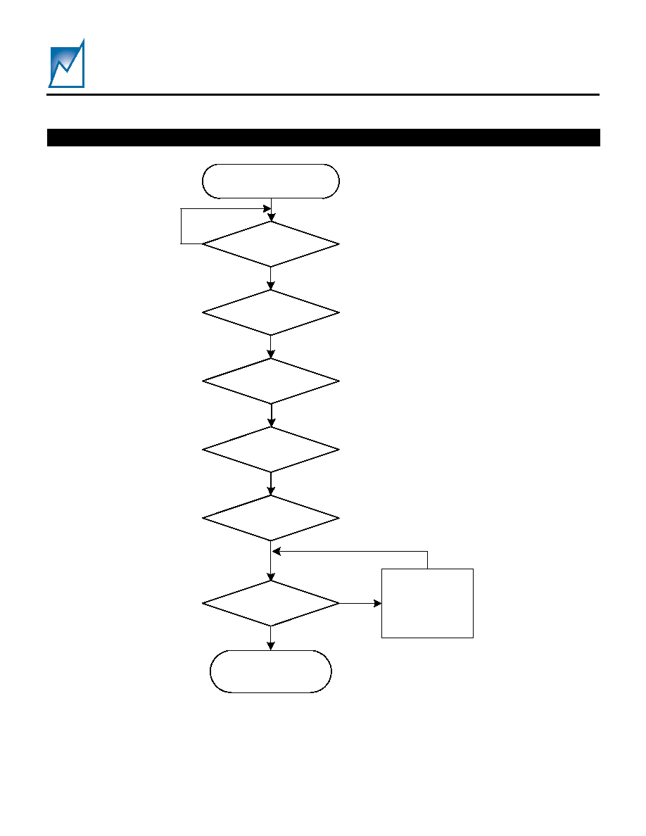
YES
POWER OK?
MARGINING OPERATION
1. HOLD DAC
2. CLEAR STATUS REGISTER
3. WAIT FOR NEXT COMMAND
INPUT VTRIM TO ADC
NO
DUMP ADC INTO DAC
DAC DRIVES BRICK
(TRIM OUTPUT LO-Z)
INPUT VOUT TO ADC
NO
ADC EQUAL TARGET?
YES
INCREMENT/
DECREMENT
DAC
Figure 5 - SMM150 Margin Flow Chart
APPLICATIONS INFORMATION (CONTINUED)

SMM150
Preliminary Information
Summit Microelectronics, Inc
2075 2.6 05/13/05
10
When measuring the delay time external to the device,
ADC sample time and Update Trim time (
4ms) must
be added to the internally programmed delay time as
shown:
Spec
Actual measurement
2.5 ms
6.5 ms
5 ms
9 ms
10 ms
14 ms
17.5 ms
22 ms
MONITOR
The SMM150 monitors the COMP1 and COMP2 pins.
COMP1 and COMP2 are high impedance inputs, each
connected internally to a comparator and compared
against the programmable internal reference voltage.
Each comparator can be independently programmed
to monitor for either UV or OV. The monitor level is
set externally with a resistive voltage divider. The
COMP pins can be connected to Vin, Vout or any
voltage that needs to be monitored. The internal
comparators COMP1/2 are compared to VREF, so the
voltage dividers are set above or below the
programmed VREF level depending on whether
monitoring UV or OV. As an example, with VREF set
to 1.25V, to monitor an OV of 1.7V on COMP1 and a
UV of 1.3V on COMP2, the voltage divider resistors
are:
For OV, RUpper = 1.37k, 1% RLower = 3.83k, 1%.
For UV, RUpper = 1.02k, 1% RLower = 25.5k, 1%.
The part can be programmed to trigger the FAULT#
pin when either COMPx comparator has exceeded the
UV or OV range. The READY and FAULT# outputs of
the SMM150 are active as long as the triggering limit
remains in a fault condition. The READY pin is
programmable active high/low open drain output
indicates that VM is at its' set point.
When programmed as an active high output, READY
can also be used as an input. When pulled low, it will
latch the state of the comparator inputs. When either
of the COMP1 or COMP2 inputs are in fault, the open-
drain FAULT# output will be pulled low. A
configuration option exists to disable the FAULT#
output while the device is in margining mode.
STATUS REGISTER
A status register exists for I
2
C polling of the status of
the COMP1 and COMP2 inputs. Two bits in this
status register reflect the current state of the inputs (1
= fault, 0 = no fault). Two additional bits show the
state of the inputs latched by one of two events
programmed in the configuration.
The first event option is the FAULT# output going
active. The second event option is the READY pin
going low. The READY pin is an I/O. As an output,
the READY output pin goes active when the DC
controlled voltages are at their set point. As an input
programmed to active high, it can be pulled low
externally and latch the state of the COMP inputs.
This second event option allows the state of the
COMP inputs on multiple devices to be latched at the
same time while a host monitors their FAULT#
outputs.
MARGINING
The SMM150 has two additional control voltage
settings: margin high and margin low. The margin
high and margin low settings can be as much as
±10%
of the nominal setting depending on the manufacturer.
The margin high and margin low voltage settings can
range from 0.3V to VDD around the converters'
nominal output voltage setting depending on the
specified margin range of the DC-DC converter. These
settings are stored in the configuration registers and
are loaded into the control voltage setting by margin
commands issued via the I
2
C bus.
The margin command registers contain two bits that
decode the commands to margin high or margin low.
Once the SMM150 receives the command to margin
the supply voltage, it begins adjusting the supply
voltage to move toward the desired setting. When this
voltage setting is reached, a bit is set in the margin
status registers and the READY signal becomes
active.
Note: Configuration writes or reads of registers 00
HEX
to 03
HEX
should not be performed while the SMM150
is margining.
FAULTS
When either of the COMP1 or COMP2 inputs are in
fault, the open-drain FAULT# output will be pulled low.
A configuration option exists to disable the FAULT#
output while the device is margining. If "Fault Output
Disabled while Margining" is selected, Faults are
disabled for all margining except when margining to
the `Off' and `Nominal' states. Also, the programmable
feature `Fault Holds Off and Shutdown Control' is
enabled only for the Nominal margin state.
APPLICATIONS INFORMATION (CONTINUED)

SMM150
Preliminary Information
Summit Microelectronics, Inc
2075 2.6 05/13/05
11
Fault Latched by a Fault Condition:
The "Fault Latched by a Fault Condition"
programmable option is triggered only on the leading
edge of a Fault. That is, a latched fault can be cleared
while the Fault yet exists.
Fault Latched by Ready I/O Pin:
Fault Latched by Ready I/O pin functions on the
margin transitions from Off to Hi/Low/Nominal or from
Nominal to Hi/Low or Hi/Low to Nominal but not from
Hi/Low/Nominal to Off.
WRITE PROTECTION
Write protection for the SMM150 is located in a volatile
register where the power-on state is defaulted to write
protect. There are separate write protect modes for the
configuration registers and memory. In order to
remove write protection, the code 55
HEX
is written to
the write protection register.
Other codes will enable write protection. For example,
writing 59
HEX
will allow writes to the configuration
register but not to the memory, while writing 35
HEX
will
allow writes to the memory but not to the configuration
registers. The SMM150 also features a Write Protect
pin (WP input) which, when asserted, prevents writing
to the configuration registers and EE memory. In
addition to these two forms of write protection there is
a configuration register lock bit which, once
programmed, does not allow the configuration
registers to be changed.
A2, A1, A0
The address bits A[2:0] can be hard wired High or Low
or may be left open (High-Z) to allow for a total of 21
distinct device addresses. When floating, the inputs
can tolerate the amount of leakage as described by
the specification I
AIT
. An external 100k pull-up or pull
down resistor is sufficient to set a High or Low logic
level.
U2
DC-DC Converter
1
2
3
4
5 6
7
8
9
10
11
+Vout
+Vout
Sense
+Vout
Gnd Gnd
+Vin
+Vin
+Vin
Trim
Enable
C10
0.1uF
READY
C7
0.01uF
R8
25.
5K 1%
Vdd
R6
3.
83K 1%
FAULT#
J2
Programming Supply
1
2
1
2
VOUT = 1.5V
U3
SMM150
1
2
3
4
5
6
7
8
9
10
11
12
13
14
15 16 17 18
19
20
21
22
23
24
25
26 27
28
SCL
A2
NC
A1
READY
A0
GND
WP
NC
CAP_M
FAULT#
COMP2
NC
VM
NC NC NC NC
COMP1
TRIM
VDD
NC
VDD_CAP
MUP
MDN
NC NC
SDA
C4
0.02uF
C3
10uF
C6
0.01uF
D1
DIODE
MDN
J1
I2C SMX3200 Connector
1
2
3
4
5
6
7
8
9
10
Gnd
SCL
Gnd3
SDA
Rsrv5
MR
+10V
Rsrv8
+5V
Rsrv10
C8
0.1uF
Vdd
R7
1.
02K 1%
C1
0.01uF
R3
20
C2
0.1uF
MUP
C5
1uF
R4 2.5k
C9
0.01uF
R5
1.
37K 1%
+VIN - 2.7V to 5.5V
Figure 6 ≠ Typical applications schematic which shows the SMM150 controlling a 3.3V in/1.5V out DC/DC
converter. Care should be taken to filter DC/DC converter noise from the SMM150 VDD supply pin. This is
accomplished with optional components R3, C1, C2, C3 and C10. This example, using a 1.25V VREF, also
shows the COMP1/2 pins monitoring the DC/DC converter VOUT set to an OV of 1.7V on COMP1 and a UV of
1.3V on COMP2, the voltage divider resistors are:
For OV, R5 = 1.37k, 1% R6 = 3.83k, 1%, For UV, R7= 1.02k, 1% R8 = 25.5k, 1%.
The jumper J2 can be used to supply the SMM150 VDD voltage from the SMX3200 programmer when the
device is programmed with board power off and the controlled supply unloaded.
APPLICATIONS INFORMATION (CONTINUED)

SMM150
Preliminary Information
Summit Microelectronics, Inc
2075 2.6 05/13/05
12
Maximizing Accuracy
Maximum margining accuracy is obtained by placing a
resistor between the SMM150 TRIM output and the
TRIM input of the converter. From the manufacturer's
data sheet obtain the value of the internal voltage
reference and equivalent TRIM input series resistance.
Figure 7 below displays the internal trimming circuit for
a typical isolated DC-DC converter. In this example,
the converter uses positive trimming, i.e., an increase
in voltage at the TRIM pin causes an increase in
output voltage.
DC-DC
Converter
TRIM
VREF
V-
V+
-S
+S
L
O
A
D
VREF
R
TRIM
SMM150
TRIM Pin
R1
R2
Figure 7 - Simplified TRIM circuit of an isolated DC-DC converter connects to SMM150 TRIM output
For this example R
TRIM
is found:
(
)
(
)
(
)
◊ -0.3
2◊
(
-0.3)
=
◊
-0.3
1-
-0.3
TRIM
VREF k
R
VREF
R
k VREF
VREF
Where:
VNom
Low
VM
)
arg(
k
=
0.3 = TRIM output saturation voltage
Vnom = Nominal (non-trimmed output voltage)
The next example applies to most non-isolated DC-DC
converters, LDO's and in-system designed converters
using monolithic PWM controllers. Figure 8 is a
simplified schematic showing the resistor divider
network used to close the loop from the output to the
circuit's feedback node. These type circuits employ
negative trimming, meaning any decrease in voltage
into the feedback node cause an increase in output
voltage.
(
)
( )
1◊
-0.3
=
◊ -1
TRIM
R
VREF
R
VNom k
VNom
High
VM
)
arg(
k
=
0.3 = TRIM output saturation voltage
Vnom = Nominal (non-trimmed output voltage)
VOUT
To FB node
(VREF)
R
TRIM
SMM150
TRIM Pin
R1
R2
Figure 8 - Simplified TRIM circuit of a non-isolated DC-DC converter connects to SMM150 TRIM output
APPLICATIONS INFORMATION (CONTINUED)

SMM150
Preliminary Information
Summit Microelectronics, Inc
2075 2.6 05/13/05
13
The end user can obtain the Summit SMX3200
programming system for device prototype
development. The SMX3200 system consists of a
programming Dongle, cable and Windows
TM
GUI
software. It can be ordered on the website or from a
local representative. The latest revisions of all
software and an application brief describing the
SMX3200 is available from the website
(
www.summitmicro.com
).
The SMX3200 programming Dongle/cable interfaces
directly between a PC's parallel port and the target
application. The device is then configured on-screen
via an intuitive graphical user interface employing
drop-down menus.
The Windows GUI software will generate the data and
send it in I
2
C serial bus format so that it can be directly
downloaded to the SMM150 via the programming
Dongle and cable. An example of the connection
interface is shown in Figure 9.
When design prototyping is complete, the software
can generate a HEX data file that should be
transmitted to Summit for approval. Summit will then
assign a unique customer ID to the HEX code and
program production devices before the final electrical
test operations. This will ensure proper device
operation in the end application.
Pin 9, 5V
Pin 7, 10V
Pin 5, Reserved
Pin 3, GND
Pin 1, GND
Pin 6, MR#
Pin 4, SDA
Pin 2, SCL
Pin 8, Reserved
Pin 10, Reserved
Top view of straight 0.1" x 0.1 closed-side
connector. SMX3200 interface cable connector.
9
7
5
3
1
10
8
6
4
2
SMM150
SDA
SCL
VDD
GND
0.1
µF
Common
Ground
WP
D1
C1
1N4148
Positive
Supply
Jumper
Figure 9≠ SMX3200 Programmer I
2
C serial bus connections to program the SMM150. The SMM150 has a
Write Protect pin (WP input) which when, asserted, prevents writing to the configuration registers and EE
memory. In addition, there is a configuration register lock bit, which, once programmed, does not allow the
configuration registers to be changed.
DEVELOPMENT HARDWARE & SOFTWARE

SMM150
Preliminary Information
Summit Microelectronics, Inc
2075 2.6 05/13/05
14
SERIAL INTERFACE
Access to the configuration registers, general-purpose
memory and command and status registers is carried
out over an industry standard 2-wire serial interface
(I
2
C). SDA is a bi-directional data line and SCL is a
clock input. Data is clocked in on the rising edge of
SCL and clocked out on the falling edge of SCL. All
data transfers begin with the MSB. During data
transfers SDA must remain stable while SCL is high.
Data is transferred in 8-bit packets with an intervening
clock period in which an Acknowledge is provided by
the device receiving data. The SCL high period (t
HIGH
)
is used for generating Start and Stop conditions that
precede and end most transactions on the serial bus.
A high-to-low transition of SDA while SCL is high is
considered a Start condition while a low-to-high
transition of SDA while SCL is high is considered a
Stop condition.
The interface protocol allows operation of multiple
devices and types of devices on a single bus through
unique device addressing. The address byte is
comprised of a 4-bit device type identifier (slave
address) and a unique (three-state) 3-bit bus address.
The remaining bit indicates either a read or a write
operation. Refer to Table 1 for a description of the
address bytes used by the SMM150. Refer to Table 2
for an example of the unique address handling of the
SMM150.
The device type identifier for the memory array, the
configuration registers and the command and status
registers are accessible with the same slave address.
It can be set using the address pins as described in
table 2.
The bus address bits A[2:0] are hard wired only
through address pins 2, 4 and 6 (A2, A1 and A0) or
may be left open (Z) to allow for a total of 21 distinct
device addresses. The bus address accessed in the
address byte of the serial data stream must match the
setting on the SMM150 address pins.
WRITE
Writing to the memory or a configuration register is
illustrated in Figures 10, 11, 12, 14, 15 and 17. A Start
condition followed by the address byte is provided by
the host; the SMM150 responds with an Acknowledge;
the host then responds by sending the memory
address pointer or configuration register address
pointer; the SMM150 responds with an acknowledge;
the host then clocks in one byte of data. For memory
and configuration register writes, up to 15 additional
bytes of data can be clocked in by the host to write to
consecutive addresses within the same page. After
the last byte is clocked in and the host receives an
Acknowledge, a Stop condition must be issued to
initiate the nonvolatile write operation.
READ
The address pointer for the configuration registers,
memory, command and status registers and ADC
registers must be set before data can be read from the
SMM150. This is accomplished by issuing a dummy
write command, which is simply a write command that
is not followed by a Stop condition. The dummy write
command sets the address from which data is read.
After the dummy write command is issued, a Start
command followed by the address byte is sent from
the host. The host then waits for an Acknowledge and
then begins clocking data out of the slave device. The
first byte read is data from the address pointer set
during the dummy write command. Additional bytes
can be clocked out of consecutive addresses with the
host providing an Acknowledge after each byte. After
the data is read from the desired registers, the read
operation is terminated by the host holding SDA high
during the Acknowledge clock cycle and then issuing a
Stop condition. Refer to Figures 13, 15 and 18 for an
illustration of the read sequence.
WRITE PROTECTION
The SMM150 powers up into a write protected mode.
Writing a code to the volatile write protection register
(write only) can disable the write protection. The write
protection register is located at address 38
HEX
. Writing
to the write protection register is shown in Figure 10.
Writing 0101
BIN
to bits [7:4] of the write protection
register allow writes to the general-purpose memory
while writing 0101
BIN
to bits [3:0] allow writes to the
configuration registers. The write protection can be re-
enabled by writing other codes (not 0101
BIN
) to the
write protection register.
I
2
C PROGRAMMING INFORMATION
SMM150
Preliminary Information
Summit Microelectronics, Inc
2075 2.6 05/13/05
15
I
2
C PROGRAMMING INFORMATION (CONTINUED)
CONFIGURATION REGISTERS
The majority of the configuration registers are grouped
with the general-purpose memory. Writing and reading
the configuration registers is shown in Figures 11, 12
and 13. See Application Note 46 for a complete
description.
Note: Configuration writes or reads of registers 00 to
03
HEX
should not be performed while the SMM150 is
margining.
GENERAL-PURPOSE MEMORY
The 256-byte general-purpose memory is located at
any slave address. The bus address bits are hard
wired by the address pins A2, A1 and A0. They can be
tied low, high or left floating, (Z). Memory writes and
reads are shown in Figures 14, 15 and 16.
COMMAND AND STATUS REGISTERS
Writes and reads of the command and status registers
are shown in Figures 17 and 18.
GRAPHICAL USER INTERFACE (GUI)
Device configuration utilizing the Windows based
SMM150 graphical user interface (GUI) is highly
recommended. The software is available from the
Summit website (
www.summitmicro.com
). Using the
GUI in conjunction with this datasheet simplifies the
process of device prototyping and the interaction of
the various functional blocks. A programming Dongle
(SMX3200) is available from Summit to communicate
with the SMM150. The Dongle connects directly to the
parallel port of a PC and programs the device through
a cable using the I
2
C bus protocol. See Figure 5 and
the SMX3200 Data Sheet.
Slave Address Bus Address Register Type
Configuration Registers are located in
00
HEX
thru 05
HEX
and 30
HEX
thru 3E
HEX
10XX
A2 A1 A0
General-Purpose Memory is located in
40
HEX
thru FF
HEX
Table 1 - Address bytes used by the SMM150.
Slave Address programmed as 10XX
Pins A[2:0]
A2 A1 A0
Slave
Address
Bus
Address
0 0 0
1000
000
0 0 1
1000
001
0 0 Z
1000
010
0 1 0
1000
100
0 1 1
1000
101
0 1 Z
1000
110
0 Z X
1000
011
1 0 0
1001
000
1 0 1
1001
001
1 0 Z
1001
010
1 1 0
1001
100
1 1 1
1001
101
1 1 Z
1001
110
1 Z X
1001
011
Z 0 0
1010
000
Z 0 1
1010
001
Z 0 Z
1010
010
Z 1 0
1010
100
Z 1 1
1010
101
Z 1 Z
1010
110
Z Z X
1010
011
Table 2 ≠ Example device addresses allowed by the SMM150.
SMM150
Preliminary Information
Summit Microelectronics, Inc
2075 2.6 05/13/05
16
S
T
A
R
T
W
A
C
K
Master
Slave
A
C
K
Configuration
Register Address = 38
HEX
0
0
1
1
1
0
0
0
0
1
0
1
0
1
0
1
S
T
O
P
Data = 55
HEX
A
C
K
A
2
Bus Address
A
1
A
0
5
HEX
Unlocks
General Purpose
EE
5
HEX
Unlocks
Configuration
Registers
Write Protection
Register Address
1
0
S
A
1
S
A
0
3
HEX
8
HEX
Figure 10 ≠ Write Protection Register Write
S
T
A
R
T
Bus Address
W
A
C
K
Master
Slave
A
C
K
Configuration
Register Address
C
7
C
6
C
5
C
4
C
3
C
2
C
1
C
0
D
7
D
6
D
5
D
4
D
3
D
2
D
1
D
0
S
T
O
P
Data
A
C
K
A
2
A
1
A
0
1
0
S
A
1
S
A
0
Figure 11 ≠ Configuration Register Byte Write
S
T
A
R
T
Bus Address
W
A
C
K
D
7
D
6
D
5
D
4
D
3
D
2
D
1
D
0
S
T
O
P
Master
Master
Slave
Slave
A
C
K
Data (16)
Configuration
Register Address
C
7
C
6
C
5
C
4
C
3
C
2
C
1
C
0
A
C
K
D
7
D
6
D
5
D
4
D
3
D
2
D
1
D
0
Data (1)
A
C
K
D
7
D
6
D
5
D
4
D
3
D
2
D
1
D
0
Data (2)
A
C
K
D
7
D
6
D
5
D
2
D
1
D
0
A
C
K
A
2
A
1
A
0
1
0
S
A
1
S
A
0
Figure 12 ≠ Configuration Register Page Write
I
2
C PROGRAMMING INFORMATION (CONTINUED)
SMM150
Preliminary Information
Summit Microelectronics, Inc
2075 2.6 05/13/05
17
S
T
A
R
T
Bus Address
W
A
C
K
D
7
D
6
D
5
D
4
D
3
D
2
D
1
D
0
S
T
O
P
N
A
C
K
Master
Master
Slave
Slave
A
C
K
Data (n)
Configuration
Register Address
C
7
C
6
C
5
C
4
C
3
C
2
C
1
C
0
S
T
A
R
T
R
A
C
K
Bus Address
A
C
K
D
7
D
6
D
5
D
2
D
1
D
0
A
C
K
D
7
D
6
D
5
D
4
D
3
D
2
D
1
D
0
Data (1)
A
2
A
1
A
0
1
0
S
A
1
S
A
0
A
2
A
1
A
0
S
A
3
S
A
2
S
A
1
S
A
0
Figure 13 - Configuration Register Read
S
T
A
R
T
Bus Address
W
A
C
K
Master
Slave
A
C
K
Configuration
Register Address
C
7
C
6
C
5
C
4
C
3
C
2
C
1
C
0
D
7
D
6
D
5
D
4
D
3
D
2
D
1
D
0
S
T
O
P
Data
A
C
K
A
2
A
1
A
0
1
0
S
A
1
S
A
0
Figure 14 ≠ General Purpose Memory Byte Write
Bus Address
S
T
A
R
T
W
A
C
K
D
7
D
6
D
5
D
4
D
3
D
2
D
1
D
0
S
T
O
P
Master
Master
Slave
Slave
A
C
K
Data (16)
Configuration
Register Address
C
7
C
6
C
5
C
4
C
3
C
2
C
1
C
0
A
C
K
D
7
D
6
D
5
D
4
D
3
D
2
D
1
D
0
Data (1)
A
C
K
D
7
D
6
D
5
D
4
D
3
D
2
D
1
D
0
Data (2)
A
C
K
D
7
D
6
D
5
D
2
D
1
D
0
A
C
K
A
2
A
1
A
0
1
0
S
A
1
S
A
0
Figure 15 - General Purpose Memory Page Write
I
2
C PROGRAMMING INFORMATION (CONTINUED)

SMM150
Preliminary Information
Summit Microelectronics, Inc
2075 2.6 05/13/05
18
S
T
A
R
T
W
A
C
K
D
7
D
6
D
5
D
4
D
3
D
2
D
1
D
0
S
T
O
P
N
A
C
K
Master
Master
Slave
Slave
A
C
K
Data (n)
Configuration
Register Address
C
7
C
6
C
5
C
4
C
3
C
2
C
1
C
0
S
T
A
R
T
R
A
C
K
A
C
K
D
7
D
6
D
5
D
2
D
1
D
0
A
C
K
D
7
D
6
D
5
D
4
D
3
D
2
D
1
D
0
Data (1)
Bus Address
Bus Address
A
2
A
1
A
0
1
0
S
A
1
S
A
0
A
2
A
1
A
0
S
A
3
S
A
2
S
A
1
S
A
0
Figure 16 - General Purpose Memory Read
S
T
A
R
T
W
A
C
K
Master
Slave
A
C
K
Command and Status
Register Address
C
7
C
6
C
5
C
4
C
3
C
2
C
1
C
0
D
7
D
6
D
5
D
4
D
3
D
2
D
1
D
0
S
T
O
P
Data
A
C
K
Bus Address
A
2
A
1
A
0
1
0
S
A
1
S
A
0
Figure 17 ≠ Command and Status Register Write
S
T
A
R
T
W
A
C
K
D
7
D
6
D
5
D
4
D
3
D
2
D
1
D
0
S
T
O
P
N
A
C
K
Master
Master
Slave
Slave
A
C
K
Data (n)
Command and Status
Register Address
C
7
C
6
C
5
C
4
C
3
C
2
C
1
C
0
S
T
A
R
T
R
A
C
K
A
C
K
D
7
D
6
D
5
D
2
D
1
D
0
A
C
K
D
7
D
6
D
5
D
4
D
3
D
2
D
1
D
0
Data (1)
Bus Address
Bus Address
A
2
A
1
A
0
S
A
3
S
A
2
S
A
1
S
A
0
A
2
A
1
A
0
1
0
S
A
1
S
A
0
Figure 18 - Command and Status Register Read
I
2
C PROGRAMMING INFORMATION (CONTINUED)

SMM150
Preliminary Information
Summit Microelectronics, Inc
2075 2.6 05/13/05
19
DEFAULT CONFIGURATION REGISTER SETTINGS ≠ SMM150NC-356
Register Contents
Function
R00 D5
Glitch filter delay time set to 120
µs.
R01
71
Nominal setting is 1.802V.
R02
9A
Margin high setting is 2.002V.
R03
48
Margin low setting is 1.602V.
R04 E0
COMP1 is UV sensor, COMP2 is OV sensor, Fault output disabled when margining,
Fault does not hold off or shutdown, Fault latched by Ready I/O Pin.
R05 28
Max converter Settling Time is 2.5ms, Margin I
2
C command enabled, MUP/MDN
pins disabled, WP is active low. VREF set to 1.25V
RC1
The default device ordering number is SMM150NC-356, is programmed as described above
and tested over the commercial temperature range. See Application Note 46 for a complete
description of the Configuration Register settings and corresponding Windows GUI
control.
SMM150
Preliminary Information
Summit Microelectronics, Inc
2075 2.6 05/13/05
20
28 Pad QFN
PACKAGE OUTLINES

SMM150
Preliminary Information
Summit Microelectronics, Inc
2075 2.6 05/13/05
21
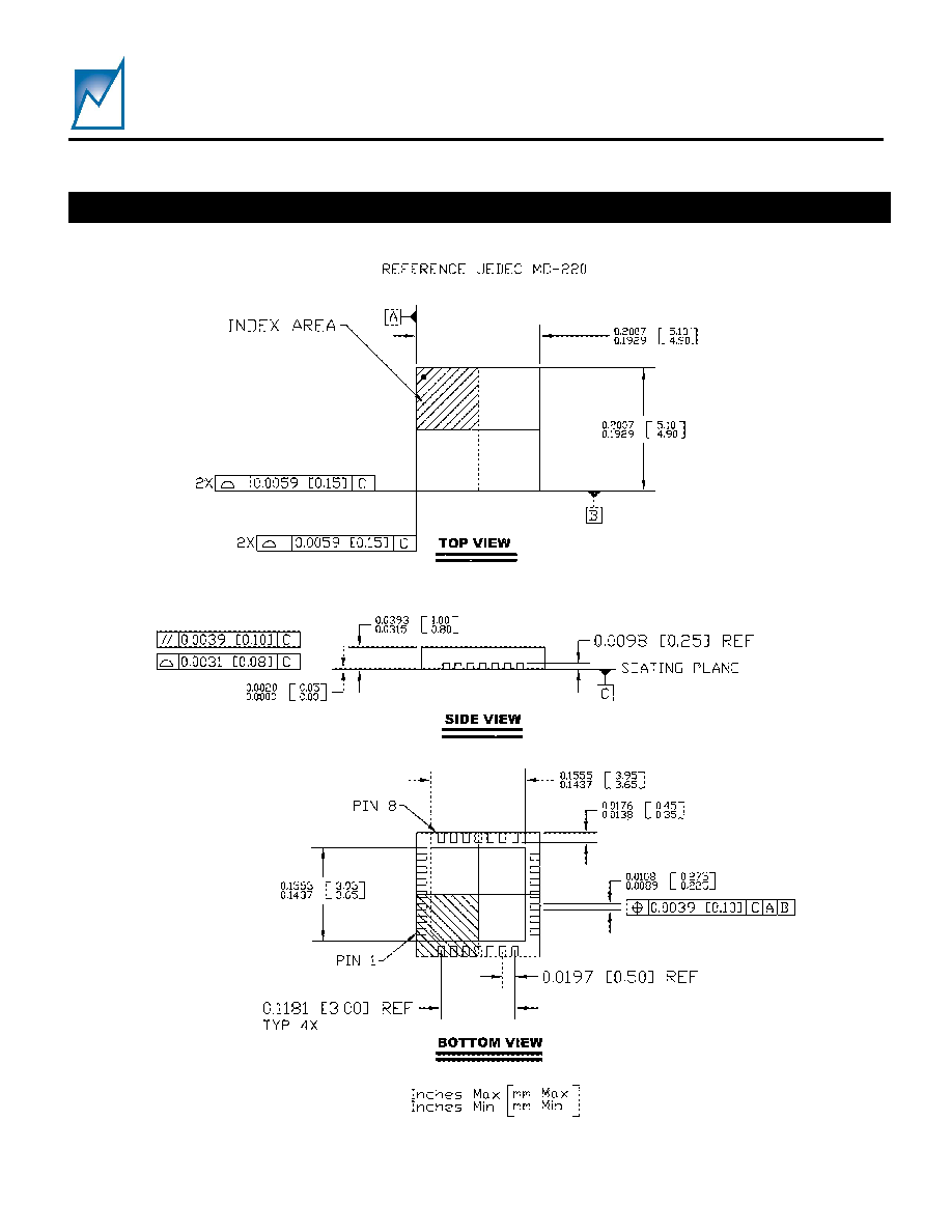
20 Ball Ultra CSP
TM
PACKAGE OUTLINES (CONTINUED)
SMM150
Preliminary Information
Summit Microelectronics, Inc
2075 2.6 05/13/05
22
PART MARKING ≠ QFN PACKAGE
SUMMIT
SMM150N
L AYYWW
Pin 1
Annn
Summit
Part Number
Date Code (YYWW)
Part Number suffix
(Contains Customer specific
ordering requirements)
Lot tracking code (Summit use)
Drawing not
to scale
SS
Status Tracking Code
(Blank, MS, ES, 01, 02,...)
(Summit Use)
Product Tracking Code (Summit use)
100% Sn, RoHS compliant, Green
ORDERING INFORMATION
NOTICE
NOTE 1 - This is a
Preliminary Information
data sheet that describes a Summit product currently in pre-production with limited characterization.
SUMMIT Microelectronics, Inc. reserves the right to make changes to the products contained in this publication in order to improve design,
performance or reliability. SUMMIT Microelectronics, Inc. assumes no responsibility for the use of any circuits described herein, conveys no license
under any patent or other right, and makes no representation that the circuits are free of patent infringement. Charts and schedules contained
herein reflect representative operating parameters, and may vary depending upon a user's specific application. While the information in this
publication has been carefully checked, SUMMIT Microelectronics, Inc. shall not be liable for any damages arising as a result of any error or
omission.
SUMMIT Microelectronics, Inc. does not recommend the use of any of its products in life support or aviation applications where the failure or
malfunction of the product can reasonably be expected to cause any failure of either system or to significantly affect their safety or effectiveness.
Products are not authorized for use in such applications unless SUMMIT Microelectronics, Inc. receives written assurances, to its satisfaction, that:
(a) the risk of injury or damage has been minimized; (b) the user assumes all such risks; and (c) potential liability of SUMMIT Microelectronics, Inc.
is adequately protected under the circumstances.
Revision 2.6 - This document supersedes all previous versions. Please check the Summit Microelectronics, Inc. web site at
www.summitmicro.com
for data sheet updates.
© Copyright 2005 SUMMIT MICROELECTRONICS, Inc.
PROGRAMMABLE ANALOG FOR A DIGITAL WORLDTM
I2C is a trademark of Philips Corporation,
Ultra
CSP
TM
is a registered name of FlipChip International, LLC.
SMM150
N
nnn
Package
Part Number Suffix (see page 19)
Summit
Part
Number
Customer specific requirements are contained
in the suffix such as Hex code, Hex code
revision, etc.
C
Temp Range
C=Commercial
Blank=Industrial
N=28 Pad QFN
E=20 Ball Ultra CSP
TM
V
is the Lead-Free Attribute for the CSP
(E Package),
L
is for the QFN (N package)
V
20 Ball Ultra CSP
TM
28 Pad QFN
SMM15
0
EV
XSSYW
W
Ball A1
Identifier
Date Code
Y = Single digit year
(4=2004, 5=2005, etc)
Drawing not
to scale
Summit Part Number
X is the sequential letter per wafer
(i.e. A for the first wafer, B for the second wafer,
C for the third wafer, etc.)
100% Sn, RoHS compliant,
Green