 | –≠–ª–µ–∫—Ç—Ä–æ–Ω–Ω—ã–π –∫–æ–º–ø–æ–Ω–µ–Ω—Ç: SMP9317S | –°–∫–∞—á–∞—Ç—å:  PDF PDF  ZIP ZIP |
SUMMIT MICROELECTRONICS, Inc. ∑ 300 Orchard City Drive, Suite 131 ∑ Campbell, CA 95008 ∑ Telephone 408-378-6461 ∑ Fax 408-378-6586 ∑ www.summitmicro.com
1
© SUMMIT MICROELECTRONICS, Inc. 1998
2031-04 12/4/98
Characteristics subject to change without notice
SUMMIT
MICROELECTRONICS, Inc.
FEATURES
∑
Digitally Controlled Electronic Potentiometer
∑
7-Bit Digital-to-Analog Converter (DAC)
≠ Independent Reference Inputs
≠ Differential Non-Linearity - +0.5LSB
≠ Integral Non-Linearity - +1LSB
∑
V
OUT
Value in EEPROM for Power-On Recall
≠ Equivalent to 128-Step Potentiometer
∑
Unity Gain Op Amp Drives
±
100
µ
A
∑
Simple Trimming Adjustment
≠ Up/Down Counter Style Operation
∑
Low Noise Operation
∑
"Clickless" Transitions between DAC Steps
∑
No Mechanical Wearout Problem
≠ 1,000,000 Stores (typical)
≠ 100 Year Data Retention
∑
Operation from +2.7V to +5.5V Supply
∑
Ultra-Low Power, 0.5mW max at +5V
Nonvolatile DACPOTTM Electronic Potentiometer
With Up/Down Counter Interface
SMP9317
OVERVIEW
The SMP9317 DACPOTTM trimmer is a 7-bit nonvolatile
DAC designed to replace mechanical potentiometers.
The SMP9317 includes a unity-gain amplifier to buffer the
DAC output and enables V
OUT
to swing from rail to rail.
The DACPOT trimmer operates over a supply voltage
range of 2.7V to 5.5V.
The SMP9317's simple up/down counter input provides
an ideal interface for automatic test equipment to dither
and monitor the V
OUT
voltage. This interface allows for
quick and consistent calibration of even the most sophis-
ticated systems.
The SMP9317 is a pin-compatible performance upgrade
for other industry nonvolatile potentiometers. The
SMP9317 offers higher resolution than these devices and
provides `clickless' transitions of V
OUT
.
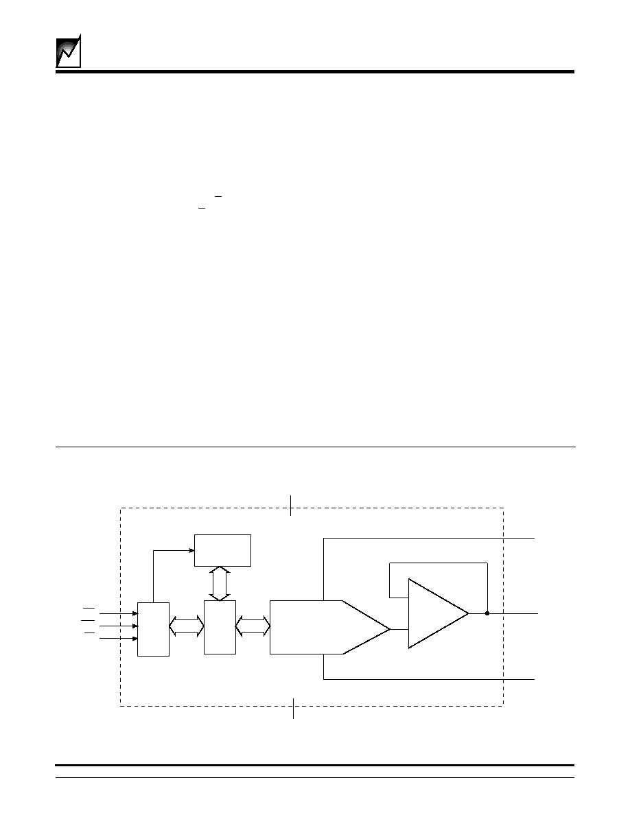
FUNCTIONAL BLOCK DIAGRAM
-
+
Counter
&
Write
Control
INC
UP/DN
CS
GND
VH
VOUT
VDD
7-bit E2 PROM
VL
7-bit
Data
Register
7-bit DAC
2031 ILL2.0
AMP
2
SMP9317
2031-04 12/4/98
Analog Section
The SMP9317 is a 7-bit, voltage output digital-to-analog
converter (DAC). The DAC consists of a resistor network
that converts a 7-bit value into equivalent analog output
voltages in proportion to the applied reference voltage.
Reference Inputs
The voltage differential between the V
L
and V
H
inputs
sets the full-scale output voltage range. V
L
must be equal
to or greater than ground (i.e. a positive voltage). V
H
must
be greater than V
L
and less than or equal to V
DD
. See
table on page 3 for guaranteed operating limits.
Output Buffer Amplifier
The voltage output is from a precision unity-gain follower
that can slew up to 1V/
µ
s.
Digital Interface
The interface is designed to emulate a simple up/down
counter, but instead of a parallel count output, a
ratiometric voltage output is provided.
Chip Select (
CS
CS
CS
CS
CS
) is an active low input. Whenever
CS
is
high the SMP9317 is in standby mode and consumes the
least power. This mode is equivalent to a potentiometer
that is adjusted to the required setting. When
CS
is low
the SMP9317 will recognize transitions on the
INC
input
and will move the V
OUT
either toward the V
H
reference or
toward the V
L
reference depending upon the state of the
UP/
DN
input.
The host may exit an adjustment routine in two ways:
deselecting the SMP9317 while
INC
is low will not per-
form a store operation (a subsequent power cycle will
recall the original data); deselecting the SMP9317 while
INC
is high will store the current V
OUT
setting into non-
volatile memory.
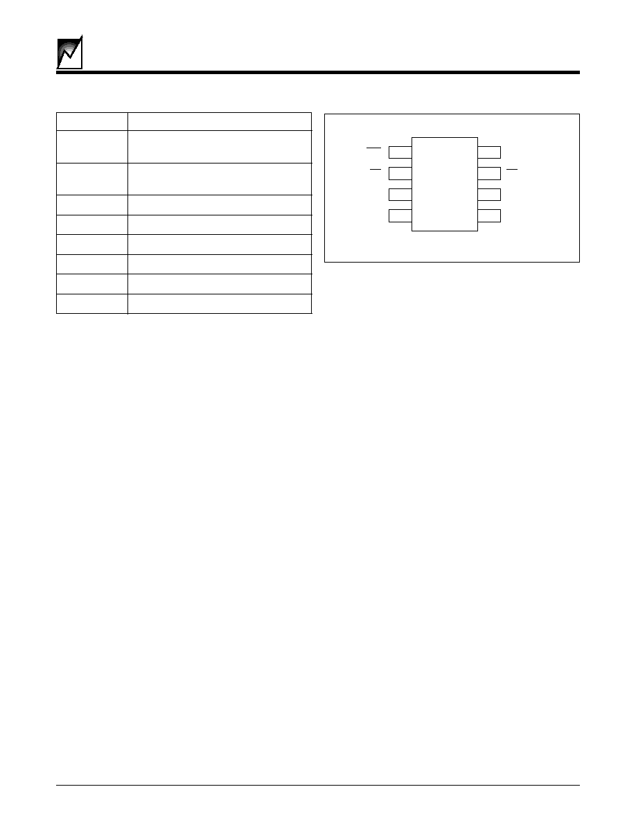
PINOUT
Increment (
INC
INC
INC
INC
INC
) is an edge triggered input. Whenever
CS
is low and a high to low transition occurs on the
INC
input, the V
OUT
voltage will either move toward V
H
or V
L
depending upon the state of the UP/
DN
input.
UP/Down (UP/
DN
DN
DN
DN
DN
) is an input that will determine the V
OUT
movement relative to V
H
and V
L
. When
CS
is low, UP/
DN
is high and there is a high to low transition on
INC
, the
V
OUT
voltage will move (1/128
th
x V
H
-V
L
) toward V
H
.
When
CS
and UP/
DN
are low, and there is a high to low
transition on
INC
, the V
OUT
will move (1/128
th
x V
H
-V
L
)
toward V
L
.
Power≠Up/Power≠Down Conditions
On power≠up the SMP9317 loads the value of EEPROM
memory into the wiper position register. The value in the
register is changed using the
CS
,
INC
, and UP/DN pins.
The new data in the register will be lost at power-down
unless
CS
was brought high, with
INC
high, to initiate a
store operation after the last increment or decrement. On
the next device power≠up, the value of EEPROM memory
will be loaded into the wiper position register. During
power-up the SMP9317 is write-protected in two ways:
1) A power-on reset, that trips at approximately 2.5V,
holds
CS
and
INC
high internally.
2) Resistor pull-ups on all logic inputs prevent data
change if the inputs are floating.
Data Retention
The SMP9317 is guaranteed to perform at least
1,000,000 writes to EEPROM before a wear≠out condi-
tion can occur. After EEPROM wearout, the SMP9317
continues to function as a volatile digital-potentiometer.
The wiper position can be changed during powered
conditions using the digital interface. However, on power≠
up the wiper≠position will be indeterminate.
On shipment from the factory, Summit Microelectronics
does not specify any EEPROM memory value. The value
must be set by the customer as needed.
PIN NAMES
Symbol
Description
INC
Increment Input, High to Low
Edge Trigger
UP/
DN
Up/Down Input controlling relative
V
OUT
movement
V
H
V+ reference input
GND
Analog and Digital Ground
V
OUT
Trimmed Voltage Output
V
L
V- reference input
CS
Active low chip select input
V
DD
Supply Voltage (2.7V to 5.5V)
INC
UP/DN
VH
GND
1
2
3
4
8
7
6
5
2031 ILL1.0
VDD
CS
VL
VOUT
SMP9317
3
2031-04 12/4/98
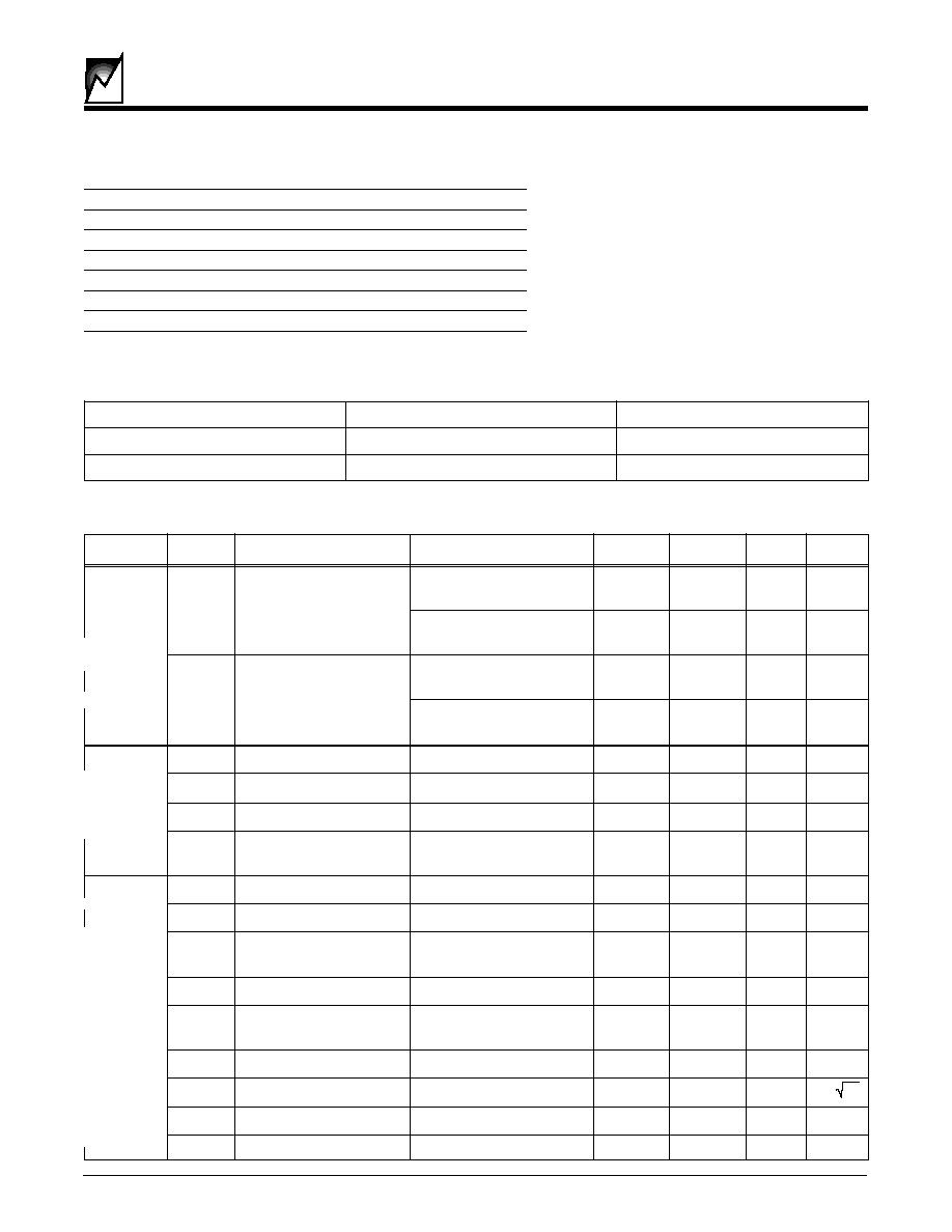
ABSOLUTE MAXIMUM RATINGS*
Temperature Under Bias
-55
∞
C to +125
∞
C
Storage Temperature
-65
∞
C to +150
∞
C
Voltage on pins with reference to GND:
Analog Inputs
-0.5V to V
DD
+.5V
Digital Inputs
-0.5V to V
DD
+.5V
Analog Outputs
-0.5V to V
DD
+.5V
Digital Outputs
-0.5V to V
DD
+.5V
Lead Solder Temperature (10 secs)
300
∞
C
*COMMENT
Stresses above those listed under Absolute Maxi-
mum Ratings may cause permanent damage to
the device. These are stress ratings only, and
functional operation of the device at these or any
other conditions outside those listed in the opera-
tion sections of this specification is not implied.
Exposure to any absolute maximum rating for
extended periods may affect device performance
and reliability.
Symbol
Parameter
Conditions
Min.
Typ.
Max.
Units
Accuracy
INL
Integral Non-Linearity
I
LOAD
= 50
µ
A,
T
R
= C
-
0.6
±
1
LSB
T
R
= I
-
0.6
±
1
LSB
I
LOAD
= 100
µ
A,
T
R
=C
-
1.2
-
LSB
T
R
= I
-
1.2
-
LSB
DNL
Differential Non-Linearity
I
LOAD
= 50
µ
A,
T
R
= C
-
0.25
±
0.5
LSB
T
R
= I
-
0.25
±
0.5
LSB
I
LOAD
= 100
µ
A,
T
R
= C
-
0.5
-
LSB
T
R
= I
-
0.5
-
LSB
References V
H
V
refH
Input Voltage
2.5
-
V
DD
V
V
L
V
refL
Input Voltage
V
H
V
L
Gnd
-
V
DD
-2.5
V
R
IN
V
refH
to V
refL
Resistance
-
38K
-
TCR
IN
Temperature Coefficient
V
refH
to V
refL
-
700
-
ppm/
∞
C
of R
IN
Analog
G
EFS
Full-Scale Gain Error
DATA = 7F
-
-
±
1
LSB
Output
V
OUT
ZS
Zero-Scale Output Voltage DATA = 00
0
20
mV
TCV
OUT
V
OUT
Temperature
V
DD
= +5, I
LOAD
= 50
µ
A,
Coefficient, note 3
V
refH
= +5V, V
refL
= 0V
-
-
200
µ
V/
∞
C
I
L
Amplifier Output Load Current
100
µ
A
R
OUT
Amplifier Output Resistance I
L
= 100
µ
A
+5V
-
10
+3V
-
20
PSRR
Power Supply Rejection
I
LOAD
= 10
µ
A
-
-
1
LSB/V
e
N
Amplifier Output Noise
f = 1KHz, V
DD
= +5V
-
90
-
nV/ H
Z
THD
Total Harmonic Distortion
V
IN
= 1V rms, f = 1KHz
-
0.08
-
%
BW
Bandwidth - 3dB
V
IN
= 100mV rms
-
1,000
-
kHz
DAC DC ELECTRICAL CHARACTERISTICS
V
DD
= +2.7V to +5.5V, V
refH
= V
DD
, V
refL
= 0V, T
A
= -40
∞
C to +85
∞
C, unless specified otherwise
2031 PGM T3.2
Condition
Min
Max
Temperature
-40
∞
C
+85
∞
C
V
DD
+2.7V
+5.5V
RECOMMENDED OPERATING CONDITIONS
2031 PGM T1.0
4
SMP9317
2031-04 12/4/98
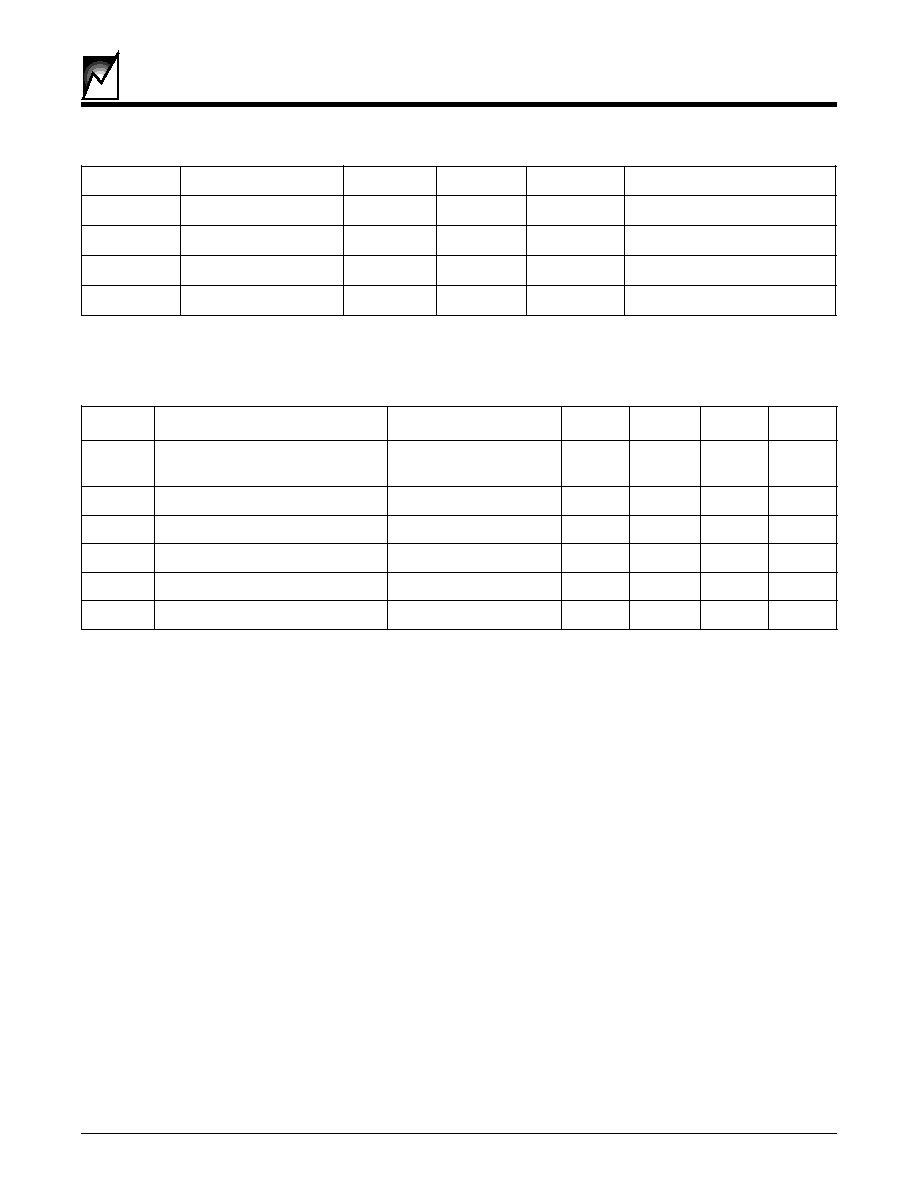
Symbol
Parameter
Min
Max
Unit
Test Method
VZAP
ESD Susceptibility
2000
V
MS-883, TM 3015
ILTH
Latch-Up
100
mA
JEDEC Standard 17
TDR
Data Retention
100
Years
MS-883, TM 1008
NEND
Endurance
1,000,000
Stores
MS-883, TM 1033
RELIABILITY CHARACTERISTICS (over recommended operating conditions unless otherwise specified)
2031 PGM T2.0
Notes:
1. I
DD
is the supply current drawn while the EEPROM is being updated. I
DD
does not include the current that flows through the Reference
resistor chain.
2.
CS
,
UP/
DN
and
INC
have internal pull-up resistors of approximately 200k
. When the input is pulled to ground the resulting output
current will be V
DD
/200k
.
3. TCV
OUT
is guaranteed but not tested.
Symbol
Parameter
Conditions
Min
Typ
Max
Units
I
DD
Supply Current
CS = V
IL
to V
IH
1.0
mA
during store, note 1
W/
INC
HI
I
SB
Supply Standby Current
CS = V
IH
100
µ
A
I
IH
Input Leakage Current
V
IN
= V
DD
10
µ
A
I
IL
Input Leakage Current, note 2
V
IN
= 0V
-25
µ
A
V
IH
High Level Input Voltage
2
V
DD
V
V
IL
Low Level Input Voltage
V
DD
4.5V
0
0.8
V
2031 PGM T4.1
DC ELECTRICAL CHARACTERISTICS
V
DD
= +2.7V to +5.5V, V
H
= V
DD
, V
L
= 0V, T
A
= -40
∞
C to +85
∞
C, Unless otherwise specified
SMP9317
5
2031-04 12/4/98
INC
INC
INC
INC
INC
CS
CS
CS
CS
CS
UP/
DN
DN
DN
DN
DN
Operation
HI
TO
LO
L
H
V
OUT
toward V
H
HI
TO
LO
L
L
V
OUT
toward V
L
H
LO
TO
HI
X
Store Setting
L
LO
TO
HI
X
Maintain Setting, NO Store
X
H
X
Standby, note 1
Notes: 1. The Standby or operating current will be lowest with
INC
and UP/
DN
pins at H as there are weak internal pull-ups that draw current
when connected LO.
2031 PGM T5.1
OPERATIONAL TRUTH TABLE
Symbol
Parameter
Min
Max
Units
t
CLIL
CS
to
INC
Setup
100
ns
t
IHDC
INC
High to UP/
DN
Change
100
ns
t
DCIL
UP/
DN
to
INC
Setup
100
ns
t
IL
INC
Low Period
200
ns
t
IH
INC
High Period
200
ns
t
IHCH
INC
Inactive to
CS
Inactive
100
ns
t
WP
Write
Cycle Time
5
ms
t
ILVOUT
INC
to V
OUT
Delay
5
µ
s
2031 PGM T6.0
AC TIMING CHARACTERISTICS
AC TIMING DIAGRAM
t
CLIL
t
IL
t
IHDC
t
IH
t
DCIL
t
IHCH
t
WP
t
ILVOUT
CS
INC
UP/DN
VOUT
2031 ILL3.1
6
SMP9317
2031-04 12/4/98
NOTICE
SUMMIT Microelectronics, Inc. reserves the right to make changes to the products contained in this publication in order to improve
design, performance or reliability. SUMMIT Microelectronics, Inc. assumes no responsibility for the use of any circuits described
herein, conveys no license under any patent or other right, and makes no representation that the circuits are free of patent
infringement. Charts and schedules contained herein reflect representative operating parameters, and may vary depending upon
a user's specific application. While the information in this publication has been carefully checked, SUMMIT Microelectronics, Inc.
shall not be liable for any damages arising as a result of any error or omission.
SUMMIT Microelectronics, Inc. does not recommend the use of any of its products in life support applications where the failure or
malfunction of the product can reasonably be expected to cause failure of the life support system or to significantly affect its safety
or effectiveness. Products are not authorized for use in such applications unless SUMMIT Microelectronics, Inc. receives written
assurances, to its satisfaction, that: (a) the risk of injury or damage has been minimized; (b) the user assumes all such risks; and
(c) potential liability of SUMMIT Microelectronics, Inc. is adequately protected under the circumstances.
© Copyright 1998 SUMMIT Microelectronics, Inc.
8 Pin SOIC (Type S) Package JEDEC (150 mil body width)
ORDERING INFORMATION
Package
S = 8 Pin SOIC
Base Part Number
SMP9317 S
2031 ILL4.0
.228 (5.80)
.244 (6.20)
.016 (.40)
.035 (.90)
.020 (.50)
.010 (.25)
x45
∞
.0192 (.49)
.0138 (.35)
.061 (1.75)
.053 (1.35)
.0098 (.25)
.004 (.127)
.05 (1.27) TYP.
.275 (6.99) TYP.
.030 (.762) TYP.
8 Places
.050 (1.27) TYP.
.050 (1.270) TYP.
8 Places
.157 (4.00)
.150 (3.80)
.196 (5.00)
1
.189 (4.80)
FOOTPRINT
8pn JEDEC SOIC ILL.2