 | –≠–ª–µ–∫—Ç—Ä–æ–Ω–Ω—ã–π –∫–æ–º–ø–æ–Ω–µ–Ω—Ç: SMP9411P | –°–∫–∞—á–∞—Ç—å:  PDF PDF  ZIP ZIP |
1
Characteristics subject to change without notice
2048 3.3 10/03/01
SMP9210, -11, -12
SUMMIT
MICROELECTRONICS, Inc.
©SUMMIT MICROELECTRONICS, Inc., 2001 ∑ 300 Orchard City Dr., Suite 131 ∑ Campbell, CA 95008 ∑ Phone 408-378-6461 ∑ FAX 408-378-6586 ∑
www.summitmicro.com
Preliminary
!
!
!
!
! Two 10-Bit Nonvolatile DACs
"
""
"
" INL ±1LSB
"
""
"
" DNL ±1LSB
!
!
!
!
! Programmable Configuration
!
!
!
!
! Programmable Power On Reset Options
"
""
"
" Recall Full Scale Value
"
""
"
" Recall Zero Scale Value
"
""
"
" Recall Mid-Scale Value
"
""
"
" Recall NV Register Value
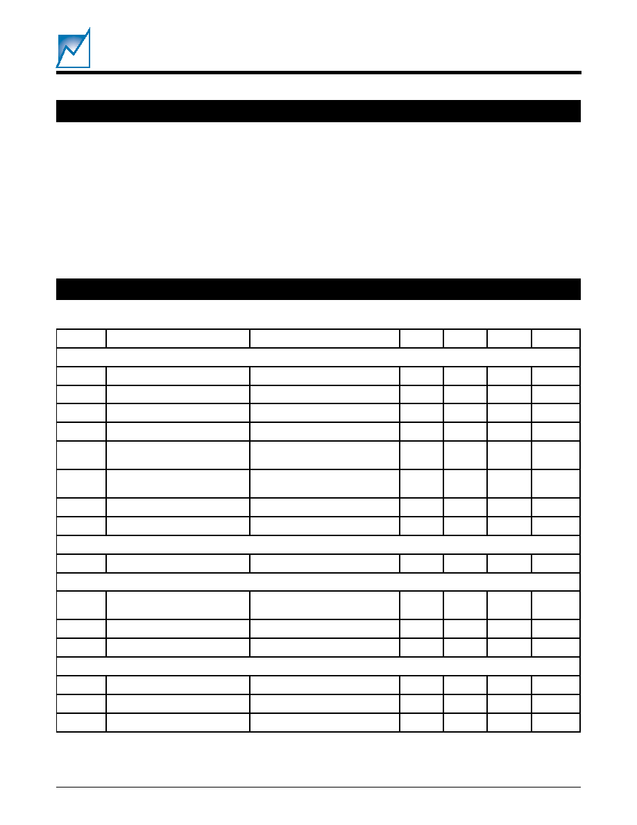
Dual 10-Bit Nonvolatile DAC
SIMPLIFIED APPLICATION DRAWING
FEATURES
CAPC
1nF
IN+
IN≠
APCSET
MODMON
MD
IMOD
Laser Driver
IBIAS
GND
MODSET
BIASSET
V
CC
APC
MONITOR
DIODE
RFILT
RDAMP
LASER
DIODE
3.3V
SMP9210
SMP9210
VOUT1
VOUT1
VOUT2
I
2
C
2048 SAD
APPLICATIONS
!
!
!
!
! ATE Set and Forget Calibration
!
!
!
!
! Laser Biasing
!
!
!
!
! Tandem or Independent Operation of DACs
!
!
!
!
! Programmable Power Down Mode (Short VOUT
to GND or Float VOUT)
!
!
!
!
! I2C Interface
!
!
!
!
! Low Noise Outputs
!
!
!
!
! 2.7V to 5.5V Operation
!
!
!
!
! ≠40∫C to 85∫C Temperature Range
!
!
!
!
! RFPA Biasing
2
SMP9210, SMP9211, SMP9212
2048 3.3 10/03/01
SUMMIT MICROELECTRONICS, Inc.
Preliminary
GND
VDD
13
7
6
VOUT2
9
SCL 12
CS
8
2048 BD10 2.2
CONFIGURATION
REGISTER
INTERFACE
& CONTROL
LOGIC
A0
3
A1 2
A2
1
SDA 14
VOLATILE
CONTROL
REGISTER
10-BIT
DAC
NON-
VOLATILE
REGISTER
VOLATILE
CONTROL
REGISTER
10-BIT
DAC
NON-
VOLATILE
REGISTER
VREFH2
4
5
11
10
VREFH1
VREFL2
VREFL1
VOUT1
SMP9210
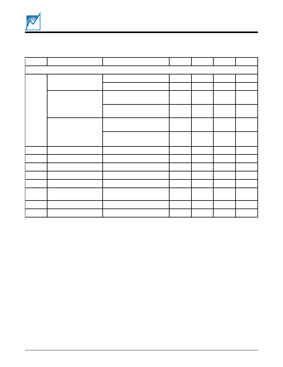
FUNCTIONAL BLOCK DIAGRAMS
Note: Pinouts for these three drawings reflect the 14 pin SOIC package.
INTRODUCTION
The SMP9210, -11, -12 trio are serial input, voltage
output, dual 10-Bit digital to analog converters. They can
operate from a single 2.7V to 5.5V supply. Internal
precision buffers swing rail-to-rail with an input reference
range from ground to the positive supply.
They integrate two 10-Bit DACs and their associated
circuits: an enhanced unity gain operational amplifier
output, a 10-Bit volatile data latch, a 10-bit nonvolatile
data register and an industry standard 2-wire serial
interface.
Programming of configuration, control and calibration
values by the user can be simplified with the interface
adapter and Windows GUI software obtainable from
Summit Microelectronics.
RECOMMENDED OPERATING CONDITIONS
Temperature
≠40
∫C to 85∫C.
Voltage
2.7V to 5.5V
3
2048 3.3 10/03/01
SMP9210, SMP9211, SMP9212
SUMMIT MICROELECTRONICS, Inc.
Preliminary
GND
VDD
13
7
6
VOUT2
9
SCL 12
2048 BD11 2.2
CONFIGURATION
REGISTER
INTERFACE
& CONTROL
LOGIC
A0
3
A1 2
A2
1
SDA 14
VOLATILE
CONTROL
REGISTER
10-BIT
DAC
NON-
VOLATILE
REGISTER
VOLATILE
CONTROL
REGISTER
10-BIT
DAC
NON-
VOLATILE
REGISTER
VREFH2
4
5
11
10
VREFH1
VREFL2
VREFL1
VOUT1
SMP9211
MUTE#
8
GND
VDD
13
7
6
VOUT2
9
SCL 12
VREF 8
2048 BD12 3.0
CONFIGURATION
REGISTER
INTERFACE
& CONTROL
LOGIC
A0
3
A1 2
A2
1
SDA 14
VOLATILE
CONTROL
REGISTER
10-BIT
DAC
NON-
VOLATILE
REGISTER
VOLATILE
CONTROL
REGISTER
10-BIT
DAC
NON-
VOLATILE
REGISTER
VREFH2
4
5
11
10
VREFH1
VREFL2
VREFL1
VOUT1
PRECISION
REFERENCE
SMP9212
4
SMP9210, SMP9211, SMP9212
2048 3.3 10/03/01
SUMMIT MICROELECTRONICS, Inc.
Preliminary
V
DD
Power supply input.
GND
Power supply return.
V
OUT
1
,
V
OUT
2
The voltage output of the DACs. It is buffered by a unity-
gain follower that can slew up to 1V/µs.
V
REF
L1, V
REF
L2
The lower of the voltage reference inputs. V
REF
L must be
equal to or greater than ground and less than V
REF
H.
V
REF
H1, V
REF
H2
The higher of the voltage reference inputs. V
REF
H must be
equal to or less than V
CC
and greater than V
REF
L.
A0, A1, A2
The address inputs for the serial interface logic. Bias-
ing the address inputs will determine the device's bus
address that is contained within the serial data stream
when communicating over the serial bus.
PIN DESCRIPTIONS
SCL
The serial interface clock. It is used to clock the data in and
out. When writing to the device data must remain stable
while SCL is high. When reading from the device data is
clocked out on the falling edge of SCL.
SDA
The bidirectional pin used to transfer data in and out of
the device.
CS
Chip Select input (V
IH
= selected) in the 9210. See the
Block Diagrams.
MUTE#
Mute input (V
IL
= mute) in the 9211. See the Block
Diagrams.
V
REF
V
REF
output (1.25V) in the 9212. See the Block Diagrams.
Note: NC pins are not connected.
PIN CONFIGURATIONS
A2
A1
A0
V
REF
H2
V
REF
L2
V
OUT
2
GND
SDA
V
DD
SCL
V
REF
H1
V
REF
L1
V
OUT
1
MUTE#
14-Pin SOIC
2048 14-PCon
1
2
3
4
5
6
7
14
13
12
11
10
9
8
A2
A1
A0
V
REF
H2
V
REF
L2
V
OUT
2
GND
SDA
V
DD
SCL
V
REF
H1
V
REF
L1
V
OUT
1
CS
1
2
3
4
5
6
7
14
13
12
11
10
9
8
A2
A1
A0
V
REF
H2
V
REF
L2
V
OUT
2
GND
SDA
V
DD
SCL
V
REF
H1
V
REF
L1
V
OUT
1
V
REF
1
2
3
4
5
6
7
14
13
12
11
10
9
8
SMP9210
SMP9211
SMP9212
1
2
3
4
5
6
7
8
16
15
14
13
12
11
10
9
2048 16-PCon
16-Pin SSOP
A2
NC
A1
A0
V
REF
H2
V
REF
L2
V
OUT
2
GND
SDA
NC
V
DD
SCL
V
REF
H1
V
REF
L1
V
OUT
1
MUTE#
SMP9210
SMP9211
SMP9212
1
2
3
4
5
6
7
8
16
15
14
13
12
11
10
9
A2
NC
A1
A0
V
REF
H2
V
REF
L2
V
OUT
2
GND
SDA
NC
V
DD
SCL
V
REF
H1
V
REF
L1
V
OUT
1
CS
1
2
3
4
5
6
7
8
16
15
14
13
12
11
10
9
A2
NC
A1
A0
V
REF
H2
V
REF
L2
V
OUT
2
GND
SDA
NC
V
DD
SCL
V
REF
H1
V
REF
L1
V
OUT
1
V
REF
5
2048 3.3 10/03/01
SMP9210, SMP9211, SMP9212
SUMMIT MICROELECTRONICS, Inc.
Preliminary
*Comment
Stresses listed under Absolute Maximum Ratings may cause perma-
nent damage to the device. These are stress ratings only, and
functional operation of the device at these or any other conditions
outside those listed in the operational sections of this specification is not
implied. Exposure to any absolute maximum rating for extended
periods may affect device performance and reliability.
Temperature Under Bias ...................... ≠55∞C to 125∞C
Storage Temperature ........................... ≠65∞C to 150∞C
Lead Solder Temperature (10 secs) .................. 300 ∞C
Terminal Voltage with Respect to GND:
V
DD
................................ ≠0.3V to 6.0V
All Others ...................... ≠0.3V to 6.0V
J
A
.................. 14 Pin = 88, 16 pin = 115
J
C
.................. 14 Pin = 37, 16 pin = 40
DC OPERATING CHARACTERISTICS
ABSOLUTE MAXIMUM RATINGS*
(Over Recommended Operating Conditions; Voltages are relative to GND)
2048 Elect TableA 3.1
(1) V
REF
L = 0.5V, V
REF
H = 4.5V
l
o
b
m
y
S
r
e
t
e
m
a
r
a
P
n
o
i
t
i
d
n
o
C
.
n
i
M
.
p
y
T
.
x
a
M
s
t
i
n
U
)
1
(
e
c
n
a
m
r
o
f
r
e
P
c
i
t
a
t
S
N
n
o
i
t
u
l
o
s
e
R
0
1
s
t
i
B
L
N
I
y
c
a
r
u
c
c
A
e
v
i
t
a
l
e
R
2
≠
1
±
2
B
S
L
L
N
D
y
t
i
r
a
e
n
il
n
o
n
l
a
i
t
n
e
r
e
f
f
i
D
c
i
n
o
t
o
n
o
m
d
e
e
t
n
a
r
a
u
G
1
≠
5
.
0
±
1
B
S
L
E
S
Z
V
r
o
r
r
e
e
l
a
c
s
o
r
e
Z
0
0
0
=
a
t
a
D
X
E
H
0
0
2
V
m
S
F
V
e
g
a
t
l
o
v
e
l
a
c
s
ll
u
F
F
F
3
=
a
t
a
D
X
E
H
V
F
E
R
H
B
S
L
1
≠
V
V
C
T
e
r
u
t
a
r
e
p
m
e
t
e
l
a
c
s
ll
u
F
t
n
e
i
c
i
f
f
e
o
c
5
1
±
m
p
p
r
o
r
r
e
t
e
s
f
f
O
3
.
0
≠
3
.
0
S
F
V
%
r
o
r
r
e
n
i
a
G
5
.
0
≠
5
.
0
%
e
c
n
a
m
r
o
f
r
e
P
g
n
i
h
c
t
a
M
r
o
r
r
e
g
n
i
h
c
t
a
m
y
t
i
r
a
e
n
i
L
5
±
B
S
L
t
u
p
t
u
O
g
o
l
a
n
A
I
T
U
O
t
n
e
r
r
u
c
t
u
p
t
u
O
0
0
2
=
a
t
a
D
X
E
H
,
V
T
U
O
,
B
S
L
3
5
±
A
m
G
E
R
D
L
e
l
a
c
s
f
l
a
h
@
n
o
i
t
a
l
u
g
e
r
d
a
o
L
0
0
2
=
a
t
a
D
X
E
H
k
1
=
L
R
,
o
t
1
4
B
S
L
C
L
d
a
o
l
e
v
i
t
i
c
a
p
a
C
n
o
i
t
a
ll
i
c
s
o
o
N
0
0
5
F
p
s
e
g
a
t
l
o
V
e
c
n
e
r
e
f
e
R
V
F
E
R
H
V
F
E
R
V
>
H
F
E
R
L
V
D
D
V
V
F
E
R
L
V
F
E
R
V
<
L
F
E
R
H
D
N
G
V
V
F
E
R
T
U
O
2
1
2
9
P
M
S
5
2
.
1
V
6
SMP9210, SMP9211, SMP9212
2048 3.3 10/03/01
SUMMIT MICROELECTRONICS, Inc.
Preliminary
2048 Elect TableB
l
o
b
m
y
S
r
e
t
e
m
a
r
a
P
n
o
i
t
i
d
n
o
C
.
n
i
M
.
p
y
T
.
x
a
M
s
t
i
n
U
r
e
w
o
P
I
D
D
t
n
e
r
r
u
c
y
l
p
p
u
s
r
e
w
o
P
V
e
t
i
r
w
V
N
D
D
V
5
.
5
=
3
A
m
V
e
t
i
r
w
V
N
D
D
V
7
.
2
=
3
A
m
t
n
e
c
s
e
i
u
q
r
o
y
b
d
n
a
t
S
h
g
u
o
r
h
t
t
n
e
r
r
u
c
g
n
i
d
u
l
c
x
E
V
s
C
A
D
D
D
V
5
.
5
=
1
A
m
h
g
u
o
r
h
t
t
n
e
r
r
u
c
g
n
i
d
u
l
c
x
E
V
s
C
A
D
D
D
V
7
.
2
=
1
A
m
n
w
o
d
r
e
w
o
P
C
A
D
g
n
i
d
u
l
c
n
i
t
n
e
r
r
u
c
l
a
t
o
T
V
D
D
V
5
.
5
=
1
A
m
C
A
D
g
n
i
d
u
l
c
n
i
t
n
e
r
r
u
c
l
a
t
o
T
V
D
D
V
7
.
2
=
1
A
m
V
D
D
e
g
a
t
l
o
v
y
l
p
p
u
S
7
.
2
5
.
5
V
V
H
I
L
C
S
,
A
D
S
7
.
0
◊
V
D
D
V
V
L
I
L
C
S
,
A
D
S
3
.
0
◊
V
D
D
V
V
L
O
A
D
S
I
L
O
A
m
3
=
4
.
0
V
I
I
L
e
g
a
k
a
e
l
t
u
p
n
I
V
N
I
o
t
0
=
V
D
D
0
0
1
A
µ
I
O
L
e
g
a
k
a
e
l
t
u
p
t
u
O
V
T
U
O
h
g
i
h
n
i
n
w
o
d
d
e
r
e
w
o
p
e
d
o
m
e
c
n
a
d
e
p
m
i
0
1
A
µ
W
D
N
E
e
c
n
a
r
u
d
n
e
e
t
i
r
W
s
n
o
i
t
a
r
e
p
o
e
r
o
t
s
V
N
f
o
r
e
b
m
u
N
1
◊
0
1
6
s
e
r
o
t
s
V
N
t
R
D
n
o
i
t
n
e
t
e
r
a
t
a
D
d
V
N
n
o
i
t
n
e
t
e
r
a
t
a
0
0
1
s
r
a
e
Y
7
2048 3.3 10/03/01
SMP9210, SMP9211, SMP9212
SUMMIT MICROELECTRONICS, Inc.
Preliminary
INTRODUCTION
The device has two 10-Bit digital to analog converters that
are comprised of a resistor network that converts a digital
input into an equivalent analog output voltage in proportion
to the applied reference voltage. The voltage differential
between each of the V
REF
L and V
REF
H input pairs sets the
full-scale output voltage for their respective DAC.
Each DAC has a 10-Bit volatile register that holds the
current digital value. The register can be set to any value
by the serial interface; commanded to load the zero scale
value, full scale value or mid-scale value; or can recall a
preset value stored in a nonvolatile register.
Each DAC has a 10-Bit nonvolatile register that can hold
a `set-and-forget' value that can be recalled whenever the
device is powered-on.
The device also has a nonvolatile configuration register
that is accessible over the 2-wire bus. The configuration
register is used to select the device type identifier, the
function of pin 8 and the DAC power-on state.
DEVICE OPERATION
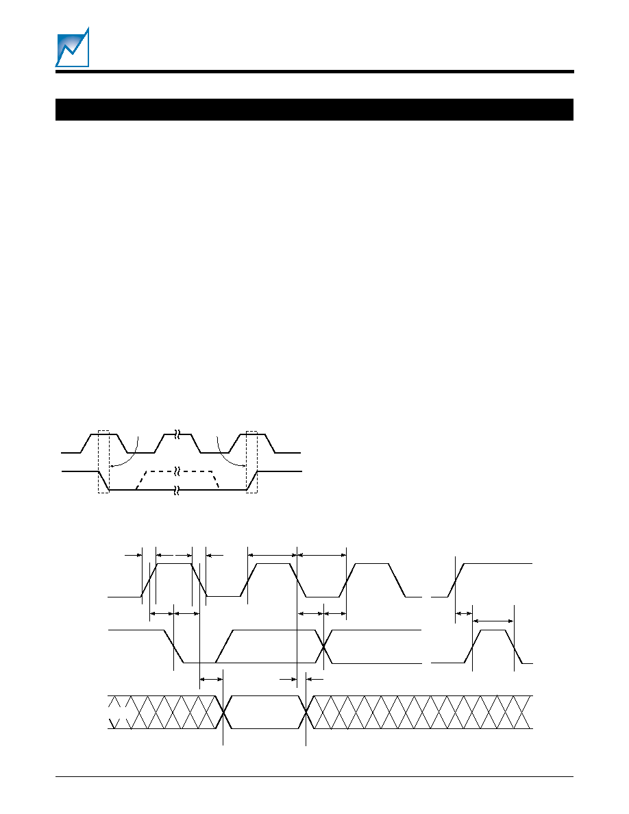
ACCESSING THE DACS
The device uses the industry standard 2-wire serial proto-
col. The bus is designed for two-way, two-line serial
communication between different integrated circuits. The
two lines are the SCL (serial clock) and SDA (serial data)
and both lines must be tied to the positive supply through
a pull-up resistor. The protocol defines devices as being
either Masters or Slaves. The SMP9210, -11, or -12 will
always be a Slave because it does not initiate any
communications or provide a clock output.
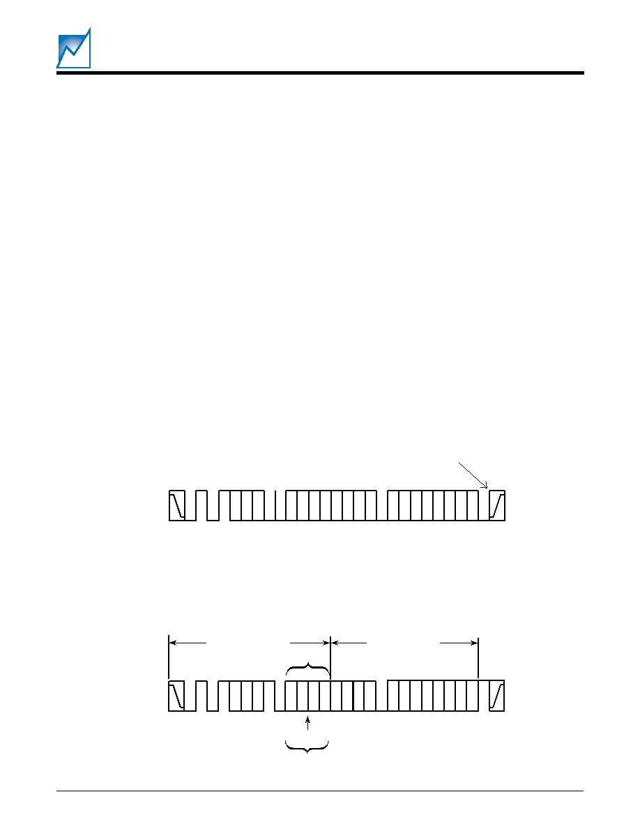
Data transfers are initiated when a Master issues a Start
condition, which is a high to low transition on SDA while
SCL is high (see Figure 1). The Start is immediately
followed by an eight bit transmission: bits 7 through 1
comprise the device type identifier and bus device bus
address; bit 0 is the Read/Write bit indicating the action
to follow. If the intended device receives the byte and
recognizes its address it will return an Acknowledge
during the 9
th
clock cycle. Some data transfers will be
concluded with a Stop condition, which is a low to high
transition on SDA while SCL is high. Note: a Stop
condition must be performed for all nonvolatile Write
operations. Timing for all I
2
C operations are summarized
in Figure 2 and Table 1.
The DAC device type identifier default is 0101
BIN
. In order
to accommodate more than eight devices on a single bus
the device type identifier can be modified by the end user
by writing to the Configuration Registers. (See page 10)
Figure 1. START and STOP Timing
Figure 2. Data/Clock Timing
2048 Fig01
SCL
SDA In
START
Condition
STOP
Condition
tF
tR
tLOW
tHIGH
tHD:STA
tSU:STA
tBUF
tDH
tHD:DAT
tSU:DAT
tSU:STO
SCL
SDA In
SDA Out
tAA
2048 Fig02
8
SMP9210, SMP9211, SMP9212
2048 3.3 10/03/01
SUMMIT MICROELECTRONICS, Inc.
Preliminary
Table 2. Command Structure
2048 Table02 3.0
Table 1. Data/Clock Timing
2048 Table01 2.0
Note (1) These values are guaranteed by design.
B
S
M
7
D
6
D
5
D
4
D
3
D
2
D
1
D
B
S
L
0
D
d
n
a
m
m
o
C
n
o
i
t
c
n
u
F
1
0
0
1
x
x
9
D
8
D
1
C
A
D
e
t
i
r
W
1
C
A
D
o
t
e
u
l
a
v
t
i
B
-
0
1
e
t
i
r
W
1
0
1
0
x
x
9
D
8
D
2
C
A
D
e
t
i
r
W
2
C
A
D
o
t
e
u
l
a
v
t
i
B
-
0
1
e
t
i
r
W
1
0
1
1
x
x
9
D
8
D
s
C
A
D
h
t
o
b
e
t
i
r
W
s
C
A
D
h
t
o
b
o
t
e
u
l
a
v
t
i
B
-
0
1
e
t
i
r
W
1
1
0
1
1
1
1
0
2
C
A
D
F
3
V
(
e
l
a
c
s
ll
u
f
o
t
2
C
A
D
t
e
S
F
E
R
)
H
1
1
0
1
1
1
0
1
1
C
A
D
F
3
V
(
e
l
a
c
s
ll
u
f
o
t
1
C
A
D
t
e
S
F
E
R
)
H
1
1
0
1
1
1
1
1
s
C
A
D
h
t
o
b
F
3
V
(
e
l
a
c
s
ll
u
f
o
t
s
C
A
D
h
t
o
b
t
e
S
F
E
R
)
H
1
1
1
0
1
1
1
0
2
C
A
D
o
r
e
Z
V
(
e
l
a
c
s
o
r
e
z
o
t
2
C
A
D
t
e
S
F
E
R
)
L
1
1
1
0
1
1
0
1
1
C
A
D
o
r
e
Z
V
(
e
l
a
c
s
o
r
e
z
o
t
1
C
A
D
t
e
S
F
E
R
)
L
1
1
1
0
1
1
1
1
s
C
A
D
h
t
o
b
o
r
e
Z
V
(
e
l
a
c
s
o
r
e
z
o
t
s
C
A
D
h
t
o
b
t
e
S
F
E
R
)
L
1
1
1
1
x
x
1
0
2
C
A
D
ll
a
c
e
R
E
ll
a
c
e
R
2
2
C
A
D
o
t
1
1
1
1
x
x
0
1
1
C
A
D
ll
a
c
e
R
E
ll
a
c
e
R
2
1
C
A
D
o
t
1
1
1
1
x
x
1
1
s
C
A
D
h
t
o
b
ll
a
c
e
R
E
ll
a
c
e
R
2
s
C
A
D
h
t
o
b
o
t
1
0
0
0
x
x
1
0
2
C
A
D
D
P
2
C
A
D
n
w
o
d
r
e
w
o
P
V
(
T
U
O
D
N
G
o
t
)
1
0
0
0
x
x
0
1
1
C
A
D
D
P
V
(
1
C
A
D
n
w
o
d
r
e
w
o
P
T
U
O
)
D
N
G
o
t
1
0
0
0
x
x
1
1
s
C
A
D
h
t
o
b
D
P
V
(
s
C
A
D
h
t
o
b
n
w
o
d
r
e
w
o
P
T
U
O
)
D
N
G
o
t
l
o
b
m
y
S
r
e
t
e
m
a
r
a
P
s
n
o
i
t
i
d
n
o
C
.
n
i
M
.
x
a
M
s
t
i
n
U
f
L
C
S
y
c
n
e
u
q
e
r
f
k
c
o
l
c
L
C
S
0
0
0
1
z
H
k
t
W
O
L
d
o
i
r
e
p
w
o
l
k
c
o
l
C
7
.
4
s
µ
t
H
G
I
H
d
o
i
r
e
p
h
g
i
h
k
c
o
l
C
0
.
4
s
µ
t
F
U
B
)
1
(
e
m
i
t
e
e
r
f
s
u
B
n
o
i
s
s
i
m
s
n
a
r
t
w
e
n
e
r
o
f
e
B
7
.
4
s
µ
t
A
T
S
:
U
S
e
m
i
t
p
u
t
e
s
n
o
i
t
i
d
n
o
c
t
r
a
t
S
7
.
4
s
µ
t
A
T
S
:
D
H
e
m
i
t
d
l
o
h
n
o
i
t
i
d
n
o
c
t
r
a
t
S
0
.
4
s
µ
t
O
T
S
:
U
S
e
m
i
t
p
u
t
e
s
n
o
i
t
i
d
n
o
c
p
o
t
S
7
.
4
s
µ
t
A
A
)
1
(
t
u
p
t
u
o
d
il
a
v
o
t
e
g
d
e
k
c
o
l
C
)
n
e
l
c
y
c
(
A
D
S
d
il
a
v
o
t
w
o
l
L
C
S
3
.
0
5
.
3
s
µ
t
H
D
)
1
(
e
m
i
t
d
l
o
h
t
u
O
a
t
a
D
e
g
n
a
h
c
A
D
S
o
t
)
1
+
n
e
l
c
y
c
(
w
o
l
L
C
S
3
.
0
s
µ
t
R
)
1
(
e
m
i
t
e
s
i
r
A
D
S
d
n
a
L
C
S
0
0
0
1
s
n
t
F
)
1
(
e
m
i
t
ll
a
f
A
D
S
d
n
a
L
C
S
0
0
3
s
n
t
T
A
D
:
U
S
)
1
(
e
m
i
t
p
u
t
e
s
n
I
a
t
a
D
0
5
2
s
n
t
T
A
D
:
D
H
)
1
(
e
m
i
t
d
l
o
h
n
I
a
t
a
D
0
s
n
I
T
)
1
(
A
D
S
d
n
a
L
C
S
r
e
t
li
f
e
s
i
o
N
n
o
i
s
s
e
r
p
p
u
s
e
s
i
o
N
0
0
1
s
n
t
R
W
e
m
i
t
e
l
c
y
c
e
t
i
r
W
5
s
m
9
2048 3.3 10/03/01
SMP9210, SMP9211, SMP9212
SUMMIT MICROELECTRONICS, Inc.
Preliminary
The command structure is illustrated in Table 2. Of
special note is the ability to write individually to either of
the two DACs, or write to them both. The first three
commands are three bytes in length and can either be
volatile or nonvolatile.
ACK and NACK
A device that is receiving data will respond with an
Acknowledge by pulling the SDA line low (ACK) after each
byte is transmitted. The transmitting device will recog-
nize this and continue to transmit. When the Master has
received the data it expects it will hold the SDA line high
(NACK) and the transmitting device will end transmis-
sion.
Sequence
The sequence is to issue a Start, followed by the device
type and bus address with the Read/Write bit set to zero.
The device will respond with an Acknowledge and the
Master will then issue the command and follow-on data.
In Figure 3 the Write is to DAC1 where the command =
1001
BIN
; D9 and D8 are the MSBs of the DAC value being
written. The device will then respond with an Acknowl-
edge followed by the Master writing the last eight bits. If
no Stop is generated after the device Acknowledge the
Write is only to the register. If the device Acknowledge
is followed by a Stop the data is written to both the DAC
register and to the nonvolatile register.
Reading the Device
Reading the DACs requires setting the R/W bit to one.
Then the host supplies clocks and the device will output
data as shown in Figure 4. PD is the Power Down mode
indicator: 1 = power down, 0= DAC active. Both DACs
provide their data for a single Read operation.
Special Configurations
The SMP9210 can be configured by the end user or by
Summit prior to shipment (see page 10). Reading the
configuration register can also be performed if it has not
already been locked. See Figure 5. There is one
configuration register and it is accessed through the serial
interface using 1001
BIN
as the device type address,
consequently the DAC address should never be set to
1001
BIN
. The register is shown in Table 3.
Figure 3. DAC1 Write Operation (see Table 2)
Figure 4. Read DAC1 (See DAC2 Differentiator & Table 2)
A
C
K
D
9
D
8
A
C
K
A
C
K
S
T
O
P
Master
SDA
Slave
0 1 0 1
R/
W
0
D
7
D
6
D
5
D
4
D
3
D
2
D
1
D
0
x
A
2
A
1
A
0
1 0 0 1
Nonvolatile Write Only
x
2048 Fig03
A
C
K
Master
SDA
Slave
0 1 0 1
R/
W
1
A
2
A
1
A
0
2048 Fig04
DAC #1
DAC #2
S
T
O
P
D
7
D
6
D
5
D
4
D
3
D
2
D
1
D
0
A
C
K
1
P
D
D
9
D
8
1 0 0 1
(1
0
1
0)
Data from Master
Data to Master
N
A
C
K
10
SMP9210, SMP9211, SMP9212
2048 3.3 10/03/01
SUMMIT MICROELECTRONICS, Inc.
Preliminary
Table 3. Configuration Register
2048 Table03 3.1
Figure 5. Configuration Register (see Table 3)
* Note: Never set the DAC address to 1001
BIN
. The Slave address for the
configuration register is 1001
BIN
, and a collision will occur on the I
2
C bus.
CONFIGURATION REGISTER
Note: All parts are normally shipped with the Configura-
tion Register locked. Unlocked user configurable parts
are available on a special order basis. Contact the
factory.
B
S
M
7
C
6
C
5
C
4
C
3
C
2
C
1
C
B
S
L
0
C
n
o
i
t
c
n
u
F
x
x
x
x
x
x
x
0
e
l
b
i
s
s
e
c
c
a
r
e
t
s
i
g
e
r
n
o
i
t
a
r
u
g
i
f
n
o
C
x
x
1
d
e
k
c
o
l
r
e
t
s
i
g
e
r
n
o
i
t
a
r
u
g
i
f
n
o
C
0
0
x
s
0
ll
a
o
t
t
e
s
s
C
A
D
:
ll
a
c
e
r
n
o
r
e
w
o
P
0
1
s
1
ll
a
o
t
t
e
s
s
C
A
D
:
ll
a
c
e
r
n
o
r
e
w
o
P
1
0
e
l
a
c
s
d
i
m
o
t
t
e
s
s
C
A
D
:
ll
a
c
e
r
n
o
r
e
w
o
P
1
1
r
e
t
s
i
g
e
r
V
N
o
t
t
e
s
s
C
A
D
:
ll
a
c
e
r
n
o
r
e
w
o
P
0
x
x
V
n
w
o
d
r
e
w
o
p
t
A
T
U
O
e
c
n
a
d
e
p
m
i
w
o
l
=
1
V
n
w
o
d
r
e
w
o
p
t
A
T
U
O
e
c
n
a
d
e
p
m
i
h
g
i
h
=
*
3
A
D
P
*
2
A
D
P
*
1
A
D
P
*
0
A
D
P
x
s
s
e
r
d
d
a
C
A
D
e
l
b
m
m
a
r
g
o
r
P
C
2
C
4
A
C
K
A
C
K
S
T
O
P
Master
SDA
Slave
1 0 0 1
R/
W
A
2
A
1
A
0
Optional
2048 Fig05
Command Byte
1
C
7
C
6
C
5
C
3
C
1
C
0
11
2048 3.3 10/03/01
SMP9210, SMP9211, SMP9212
SUMMIT MICROELECTRONICS, Inc.
Preliminary
ORDERING INFORMATION
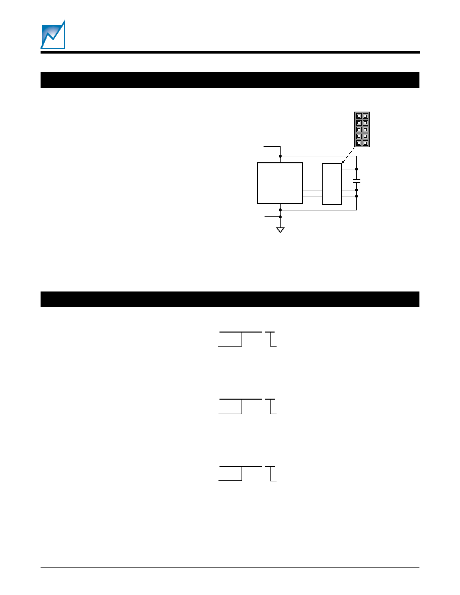
PROGRAMMING CONNECTION
Figure 6. Programming Connection
HARDWARE
The end user can use the summit SMX3200 programming
cable and software that have been developed to operate
with a standard personal computer. The programming
cable interfaces directly between a PC's parallel port and
the target application. The application's values are
entered via an intuitive graphical user interface employing
drop-down menus.
After the desired settings for the application are deter-
mined the software will generate a hex file that can be
transferred to the target device or downloaded to Summit.
If it is downloaded to Summit a customer part number will
be assigned and the file will be used to customize the
devices during the final electrical test operations.
SMP9210 S
Base Part Number
Package
S = SOIC
G = SSOP
2048 Tree
SMP9211 S
Base Part Number
Package
S = SOIC
G = SSOP
SMP9212 S
Base Part Number
Package
S = SOIC
G = SSOP
Pin 9, 5V
Pin 7, 10V
Pin5, Reserved
Pin3, GND
Pin 1, GND
Pin 10, Reserved
Pin 8, Reserved
Pin 6, Reserved
Pin 4, SDA
Pin 2, SCL
Top view of straight 0.1"
◊
0.1" closed
side connector SMX3200 interface
Positive
Supply
Negative
Supply
VDD
GND
A0
A1
A2
SDA
SCL
9
7
5
3
1
10
8
6
4
2
SMP92xx
2048 Fig06
C1
0.1µF
12
SMP9210, SMP9211, SMP9212
2048 3.3 10/03/01
SUMMIT MICROELECTRONICS, Inc.
Preliminary
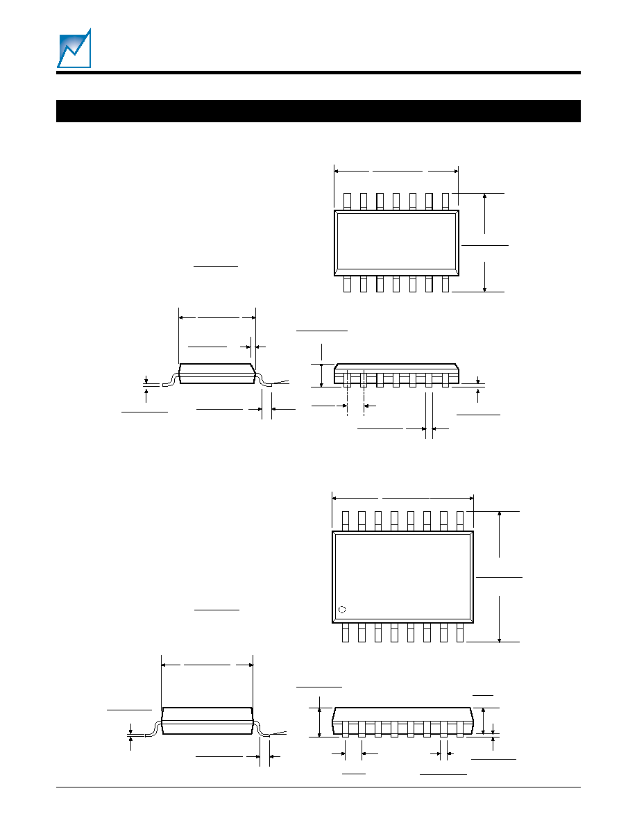
PACKAGES
14 PIN SOIC PACKAGE
0.150 - 0.157
0.013 - 0.020
(0.33 - 0.51)
0.004 - 0.01
(0.10 - 0.25)
0.337 - 0.344
(8.55 - 8.75)
0.228 - 0.244
(5.80 - 6.20)
0.053 - 0.069
(1.35 - 1.75)
0.016 - 0.050
(0.40 - 1.27)
(1.27)
0.0075 - 0.01
(0.19 - 0.25)
0.01 - 0.02
(0.25 - 0.50)
(3.80 - 4.00)
14 Pin SOIC
◊
45
∫
0.016 - 0.050
0.05
0 to 8
typ
1
Ref. JEDEC MS-012
Inches
(Millimeters)
0.007 - 0.010
(0.18 - 0.25)
0.150 - 0.157
(3.81 - 3.99)
0.025
(0.635)
0.016 - 0.050
(0.41 - 1.27)
0.008 - 0.012
(0.20 - 0.31)
0.189 - 0.197
(4.80 - 5.00)
0.228 - 0.244
(5.79 - 6.20)
Pin 1
0
∫
to 8
∫
0.004 - 0.010
(0.10 - 0.25)
0.059
(1.50)
0.053 - 0.069
(1.35 - 1.75)
MAX
16 Pin SSOP
Ref. JEDEC MO-137
Inches
(Millimeters)
16 PIN SSOP PACKAGE
13
2048 3.3 10/03/01
SMP9210, SMP9211, SMP9212
SUMMIT MICROELECTRONICS, Inc.
Preliminary
NOTICE
SUMMIT Microelectronics, Inc. reserves the right to make changes to the products contained in this publication in order
to improve design, performance or reliability. SUMMIT Microelectronics, Inc. assumes no responsibility for the use of
any circuits described herein, conveys no license under any patent or other right, and makes no representation that
the circuits are free of patent infringement. Charts and schedules contained herein reflect representative operating
parameters, and may vary depending upon a user's specific application. While the information in this publication has
been carefully checked, SUMMIT Microelectronics, Inc. shall not be liable for any damages arising as a result of any
error or omission.
SUMMIT Microelectronics, Inc. does not recommend the use of any of its products in life support or aviation applications
where the failure or malfunction of the product can reasonably be expected to cause any failure of either system or to
significantly affect their safety or effectiveness. Products are not authorized for use in such applications unless
SUMMIT Microelectronics, Inc. receives written assurances, to its satisfaction, that: (a) the risk of injury or damage has
been minimized; (b) the user assumes all such risks; and (c) potential liability of SUMMIT Microelectronics, Inc. is
adequately protected under the circumstances.
Power Management for CommunicationsTM
© Copyright 2001 SUMMIT Microelectronics, Inc.
This Document supersedes all previous versions.
I2C is a trademark of Philips Corporation.
PART MARKING
n
= Package type (P or S)
L
= Lot number
YY
= Year
WW
= Work Week
9210:
ZZ
= blank
9211:
ZZ
= 11
9212:
ZZ
= 12
.
SUMMIT
SMP9210
n
L YY WW
ZZ