 | –≠–ª–µ–∫—Ç—Ä–æ–Ω–Ω—ã–π –∫–æ–º–ø–æ–Ω–µ–Ω—Ç: SMS64FR03 | –°–∫–∞—á–∞—Ç—å:  PDF PDF  ZIP ZIP |
SMS64
Preliminary
©
SUMMIT MICROELECTRONICS, Inc. 2003 ∑ 1717 Fox Dr. ∑ San Jose, CA 95131 ∑ Phone 408-436-9890 ∑ FAX 408-436-9897 ∑
wwwsummitmicro.com
Characteristics Subject to Change Without Notice
2060 2.22 10/09/03
1
FEATURES & APPLICATIONS
∑ Monitors and Controls up to 6 Power
Supplies
∑ Programmable Sequencing for both Power-
on and Power-off
∑ Programmable Threshold Sensors
∑ Programmable Reset and Interrupt Functions
∑ Programmable Watchdog/Longdog Timer
∑ Fault and Status Registers
∑ 4k-Bit Nonvolatile Memory
Applications
∑ Monitor and Control Distributed Power and
Point of Use Power Supplies
∑ Telecom
∑ Compact PCI
∑ Servers
∑ Multi-voltage Network Processors, DSPs,
ASICs
INTRODUCTION
The SMS64 is a highly integrated power supply
monitor and controller. The SMS64 has six supply
managers, each individually programmable with
regard to threshold voltages, actions that can be taken
with either an under- or over-voltage condition and
how that manager will operate in sequencing the
power-on operation.
The managers can act independently or sequenced
with any other manager in the device. When the
managers work together the device can control the
sequence in which power is applied to the application
circuits. Each manager is assigned to a sequence
position which allows the device to perform power
supply sequencing in any order. For power-off
situations the SMS64 can sequence the supplies
either in the same order or reverse order from the
power-on sequence.
The SMS64 has two programmable Watchdog
timers, two programmable reset outputs and a
programmable IRQ# output. Using the I
2
C 2-wire
serial interface, a host system can communicate with
the SMS64 status register, optionally control power-on
via software and utilize 4 K-bits of nonvolatile memory.
Six-Channel Supply Monitor and Sequencing Controller
GND
V+
OUT
SET
ON/OFF
GND
V+
OUT
ON/OFF
GND
V+
OUT
SET
SHDN
3.3V
2.7V
VC
C
A
PU
P
A
VM
A
VC
C
B
PU
P
B
VM
B
PU
P
C
VM
C
PUP
D
VM
D
PU
P
F
VM
F
PU
P
E
VM
E
ASIC
DSP
2.5V
1.8V
2.0V
1.5V
H
E
A
L
T
H
Y
#
IR
Q
#
RST_A#
RS
T
_
B
#
VCC_CAP
G
N
D
Pow er-On
IRQ#
HEALTHY#
GND
V
G
G
_C
A
P
MR#
RESET#
SMS64
GND
V+
OUT
ON/OFF
PW R_ON/OFF
2.7V
2.7V
UP
Power Supply Sequencing and System Start-up Initialization using the SMS64
This is an example application and the specific component values are purposely not shown. The SMS64 can be used with any combination of
MOSFETs, LDOs or DC/DC converters to optimize sequencing and minimize losses in the power chain.
SIMPLIFIED APPLICATIONS DRAWING
SMS64
Preliminary
Summit Microelectronics, Inc
2060 2.22 10/09/03
2
GENERAL DESCRIPTION
The SMS64 has four major functional blocks; the
supply managers and the sequencing outputs; the
programmable reset and interrupt circuitry; the timing
and control block; and the nonvolatile memory array.
The managers are comprised of a voltage monitor
with a programmable threshold input. The monitored
voltage threshold can be programmed anywhere
between 0.9V and 6.0V in 20mV increments. Each
monitor provides an under-voltage/over-voltage
(UV/OV) signal to the internal bus.
Associated with each monitor is an output circuit
(PUP circuit) that can be used to enable or switch an
external power supply to the application's circuits. The
point in time and position in a sequence when the
output is asserted is programmable and is controlled
by the sequence position assignments and the PUP
delays in the timing and control block.
The other major block is a programmable reset and
interrupt block. The SMS64 provides a great deal of
flexibility in choosing the trigger source for the resets
and interrupt. The sources include multiple
combinations of UV/OV conditions, and programmable
Watchdog and Longdog timers.
Programming of the SMS64 is performed over the
industry standard I
2
C, 2-wire serial data interface. It
allows configuration of the device, real-time control of
the power-on/power-off processes and instant-access
to the power supply status of the application circuit.
The bus interfaces the host to 4k bits of nonvolatile
memory and the programmable configuration
registers.
2.5V
2.7V
1.8V
---
t2
---
RST_B#
RST_A#
2.0V
1.5V
3.3V
Figure 1 ≠ Example Power Supply Sequencing and System Start-up Initialization using the SMS64 as
shown in the Simplified Applications Drawing on page 1. Any order of supply sequencing can be applied
using the SMS64
SMS64
Preliminary
Summit Microelectronics, Inc
2060 2.22 10/09/03
3
FUNCTIONAL BLOCK DIAGRAM
PUP
Control B
Voltage
Monitor A
PUP
Control A
PUP
Control C
UV/OV
A
VCC
A
VM
A
Voltage
Monitor B
UV/OV
B
VCC
B
VM
B
Voltage
Monitor C
UV/OV
C
VCC
C
VM
C
Reset and
Interrupt
Control
Logic
RST_A#
IRQ#
W LDI
M R#
HEALTHY#
RST_B#
PUP
C
PUP
B
PUP
A
I
2
C Serial
Interface
SCL
SDA
13
14
11
10
A2
A1
Sequence
Control
PUP
Control E
Voltage
Monitor D
PUP
Control D
PUP
Control F
UV/OV
D
VCC
D
VM
D
Voltage
Monitor E
UV/OV
E
VCC
E
VM
E
Voltage
Monitor F
UV/OV
F
VCC
F
VM
F
PUP
F
PUP
E
PUP
D
Power
Supply
Arbitration
VGG_CAP
VCC_CAP
24
GND GND
12
CS#
6
31
5
32
4
33
3
34
2
35
1
36
7
37
28
26
18
30
25
27
46
45
43
16
FS#
42
41
40
Memory
Array
17
PW R_ON/OFF
15
100K
100K
100K
100K
VCC_CAP
VCC_CAP
SMS64
Preliminary
Summit Microelectronics, Inc
2060 2.22 10/09/03
4
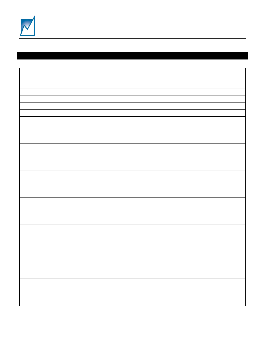
PIN DESCRIPTIONS
Pin
Number
Pin
Type
Pin Name
Pin Description
6 PWR VCC
A
5 PWR VCC
B
4 PWR VCC
C
3 PWR VCC
D
2 PWR VCC
E
1 PWR VCC
F
The VCC inputs have two functions on the SMS64. They are used as the
power supply inputs and as such are diode-OR'ed so that at any point in time the
highest potential input will be the power source for the SMS64. So long as one of
the inputs is at or above 1V the RESET outputs will be active. For proper device
operation, including sequencing, at least one of the pins must be at or above
2.7V.
Each VCC input can be programmed as a voltage sensing input. It will only be
used as a precursor to power-on sequencing. Once it reaches its V
PTH
the
comparator's source input will be switched to its corresponding VM input.
7 PWR
VCC_CAP VCC_CAP is a charge storage connection to the SMS64's internal power
supply. For most applications this pin is tied to a 10µF capacitor.
10 I A2
11 I A1
The address pins are biased either to VCC_CAP or GND. When
communicating with the SMS64 over the 2-wire bus these pins provide a
mechanism for assigning a unique bus address. A2 and A1 are internally
connected to VCC through a 100K
resistor.
12 I CS#
The Chip Select input is used solely for enabling communication on the 2-wire
bus. In order to write or read the registers or the memory array the CS# input
must be low. CS# is internally connected to VCC through a 100K
resistor.
13 I SCL
The SCL input is used to clock data into and out of the memory array. In the
write mode, data must remain stable while SCL is HIGH. In the read mode, data
is clocked out on the falling edge of SCL.
14 I/O SDA
SDA is the bidirectional serial data pin. It is configured as an open drain
output and will require a pull-up resistor to VCC_CAP or a higher potential system
supply.
15 PWR GND
GND is the ground for both the analog and digital portions of the internal
circuitry. It is internally tied to pin 24. (Both pins should be tied to system ground).
16 I FS# The force shutdown input is used to immediately turn off all PUP outputs. FS#
is internally connected to VCC through a 100K
resistor.
17 I
PWR_
ON/OFF
The PWR_ON/OFF input is used to initiate power-on and power-off
sequencing. When the input is high and all of the programmed preconditions are
met, the SMS64 will power-on.
If the input is taken low, the SMS64 will begin the power-off operation. If
programmed to do so, the SMS64 will sequence off the PUP outputs either in the
power-on order or reverse order. PWR_ON/OFF is internally connected to VDD
through a 100K
resistor.
18 I MR#
MR# is the manual reset input. When MR# is taken low the RST_A# and
RST_B# outputs will be driven low. The RST outputs will stay low so long as the
MR# input is low, and will remain low for t
PRTO
after MR# returns high (so long as
no other reset conditions exist).
MR# must be low in order to write to the configuration registers and high to
write to the memory array (see descriptions on page 16).
MR# is internally
connected to VCC through a 100k
pull-up resistor.
PIN DESCRIPTIONS
SMS64
Preliminary
Summit Microelectronics, Inc
2060 2.22 10/09/03
5
Pin
Number
Pin
Type
Pin Name
Pin Description
24 PWR GND
GND is the ground for both the analog and digital portions of the internal
circuitry. It is internally tied to pin 15. (Both pins should be tied to system ground).
25 O IRQ#
The interrupt output is an active low open-drain output. It will be driven low
whenever the Watchdog timer times out or whenever an enabled under-voltage or
over-voltage condition on a VM input exists.
The IRQ# signal is held in an inactive state during the power-on and
power-off sequence.
26 O
RST_B#
During the power-on sequence RST_B# will be asserted (driven low) until the
entire power-on sequence has been completed and the programmable reset
interval timer (tPRTO) has elapsed.
RST_B# will be forced low by asserting the MR# input. It will remain low so long
as the MR# input is low plus the programmed reset time out period for RST_B#.
RST_B# will be asserted whenever an enabled UV/OV condition exists.
RST_B# will remain active so long as the UV/OV condition exists and t
PRTO
expires.
The RST_B# is an active low open drain output.
27 O
RST_A#
During the power-on sequence RST_A# will be driven low and will remain low
until a selected PUP output has become active. and the triggers for RST_A# are
inactive. In this manner the RST_A# can be used to release a portion of the circuitry
from reset before the entire system is energized.
RST_A# will be forced low by asserting the MR# input. It will remain low so long
as the MR# input is low plus the programmed reset time out period for RST_A#.
RST_A# will be asserted whenever an enabled UV/OV condition exists.
RST_A# will remain active so long as the UV/OV condition exists and t
PRTO
expires.
The RST_A# is an active low open drain output.
28 O
HEALTHY#
The healthy output is used to signal that the VM inputs are not generating any
under-voltage or over-voltage conditions.
30 I WLDI
WLDI is the Watchdog and Longdog timers' interrupt input. A low to high
transition on the WLDI input will clear both the Watchdog and Longdog timers,
effectively starting a new time-out period.
If WLDI is stuck low and no low-to-high transition is received within the
programmed t
PWDTO
period (programmed watch dog time-out) IRQ# will be driven
low. If a transition is still not received within the programmed t
PLDTO
period
(programmed Longdog time-out) RESET# will be driven low. Refer to Figure 5 for a
detailed illustration.
Holding WLDI high will block interrupts from occurring but will not block the
Longdog from timing out and generating a reset. Refer to Figure 3 for a detailed
illustration of the relationship between IRQ#, RESET#, and WLDI.
31 I VM
A
32 I VM
B
33 I VM
C
34 I VM
D
35 I VM
E
36 I VM
F
The VM pins are the voltage monitor inputs. The input voltage is either
compared to a programmed threshold voltage (V
PTH
) or it can be compared to a
preset reference voltage of 0.5V.
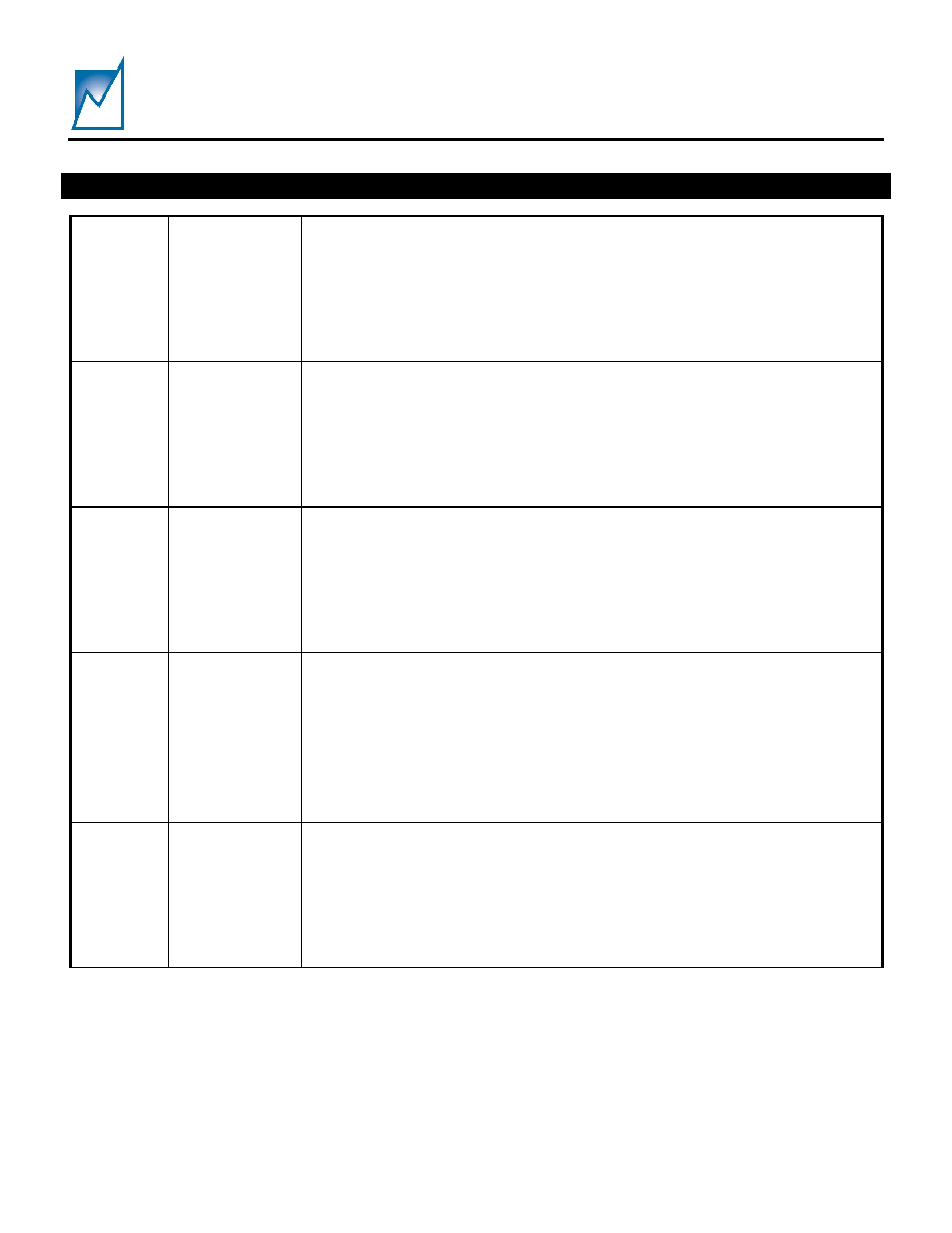
PIN DESCRIPTIONS CONT'D
SMS64
Preliminary
Summit Microelectronics, Inc
2060 2.22 10/09/03
6
Pin
Number
Pin
Type
Pin Name
Description
37 PWR VGG_CAP
VGG_CAP is a charge storage connection for the internal charge pump
of the SMS64. This capacitor should be of sufficient size so as to provide
current, under varying load conditions, to the PUP outputs that are
programmed as high side drivers. For most applications this can be tied to a
01
µF capacitor.
40 O
PUP
F
41 O
PUP
E
42 O
PUP
D
43 O
PUP
C
45 O
PUP
B
46 O
PUP
A
The points of use power enable (PUP) outputs are used when cascading
or sequencing external supplies such as LDO's DC-to-DC converters or
MOSFETs.
The output can be configured as an open drain active high or active low
output. In both configurations an external pull-up resistor is required.
The output can also be configured as a high-side driver output. The
output voltage for this configuration can be set at 10.5V or 14.5V.
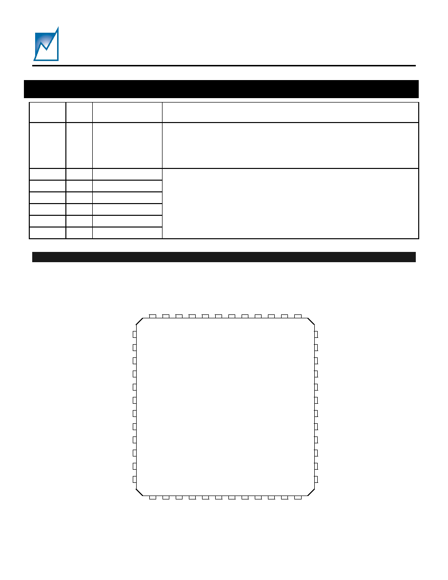
PACKAGE & PIN CONFIGURATION
48 PIN TQFP
1
2
3
4
5
6
7
8
9
10
11
12
13
14
15
16
17
18
19
20
21
22
23
24
36
35
34
33
32
31
30
29
28
27
26
25
48
47
46
45
44
43
42
41
40
39
38
37
SMS64
VM
E
PU
P
A
PU
P
C
PU
P
D
PU
P
B
PU
P
E
VM
D
VM
C
VM
F
VM
B
VM
A
PU
P
F
VCC
A
VCC
C
VCC
B
VCC
D
VCC
F
VCC
E
VCC_CAP
A2
A1
CS#
SD
A
SC
L
FS#
MR
#
GND
GND
HEALTHY#
RST_A#
RST_B#
IRQ#
V
G
G_CAP
WLDI
PW
R
_
O
N
/O
FF
PIN DESCRIPTIONS CONT'D
SMS64
Preliminary
Summit Microelectronics, Inc
2060 2.22 10/09/03
7
ABSOLUTE MAXIMUM RATINGS
Temperature Under Bias ...................... -55
∞
C to 125
∞
C
Storage Temperature............................ -65
∞
C to 150
∞
C
Terminal Voltage with Respect to GND:
VCC
A
, VCC
B
, VCC
C
, VCC
D
, VCC
E
, VCC
F
..-0.3V to 6.0V
VM
A
, VM
B
, VM
C
, VM
D
, VM
E
, VM
F
...............-0.3V to 6.0V
PUP
A
, PUP
B
, PUP
C
, PUP
D,
PUP
E
, PUP
F
.............. 15.5V
All Others ......................................................V
CC
+ 0.7V
Output Short Circuit Current ............................... 100mA
Lead Solder Temperature (10 secs).................... 300
∞
C
ESD Rating per JEDEC................................2000V
Latch-Up testing per JEDEC.....................+/- 100mA
RECOMMENDED OPERATING CONDITIONS
Temperature Range(Ambient).........-40
∞
C to +85
∞
C
Supply Voltage...............................2.7V to 6.0V
1/
Package Thermal Resistance (
JA)
48 Lead SSOP.......................................80
o
C/W
Moisture Classification Level 1 (MSL 1) per J-STD- 020
RELIABILITY CHARACTERISTICS
Data Retention.....................................100 Years
Endurance...................................100,000 Cycles
Stresses listed under Absolute Maximum Ratings may cause permanent
damage to the device. These are stress ratings only and functional operation
of the device at these or any other conditions outside those listed in the
operational sections of the specification is not implied. Exposure to any
absolute maximum rating for extended periods may affect device performance
and reliability. Devices are ESD sensitive. Handling precautions are
recommended.
DC OPERATING CHARACTERISTICS
(Over recommended operating conditions, unless otherwise noted. All voltages are relative to GND.)
Symbol Parameter
Notes
Min.
Typ.
Max
Unit
VCC
Supply Voltage VCC
A
, VCC
B
, VCC
C,
VCC
D,
VCC
E,
VCC
F
Device supply voltage
defined by the highest of
the six VCC inputs. Must
be > 2.7V. ≠ Note 1/
2.7 6.0
V
I
DD
(ON)
Active Current with PUP
Outputs configured as
high-side drivers enabled
2
mA
I
DD
(Off)
Power Supply Current
Quiescent Current high-
side PUP Outputs disabled
1
mA
P
VIT
Programmable Threshold (VCC and VM
Inputs)
8-bit resolution 20mV/bit
0.9
6.0
V
V
TH
Fixed threshold Voltage
"naked" mode, V input
disconnected from ground
0.5 V
PUP characteristics when configured as high-side driver
Option 1 (MOSFETs on)
14.5
V
P
VPUP
Programmable PUP Output
Option 2 (MOSFETs on)
10.5
V
V
PUP
OFF PUP Output
I
PUPSINK
= 2mA
0
0.4
V
I
PUP
PUP Drive Current
When configured as high-
side driver and with
MOSFET switches on
8
µA
SR
PUP
PUP Slew Rate
When Configured as High
Side Driver
250 V/s
PUP characteristics when configured as a logic output
V
OL
Output Low Voltage
I
SINK
= 2mA
0
0.4
V
All other input and output characteristics
VCC = 2.7V
0.9xVI
VI
V
V
IH
Input High Voltage (FS#, PWR_ON/OFF,
MR#)
VCC = 5.0V
0.7xVI
VI
V
VCC = 2.7V
-0.1
0.1xVI
V
V
IL
Input Low Voltage (FS#, PWR_ON/OFF,
MR#)
VCC = 5.0V
-0.1
0.3xVI
V
V
OL
Open Drain Outputs (RST_A#, RST_B#,
IRQ#, HEALTHY#)
I
SINK
= 2mA
0
0.4
V
Notes: 1/ At least one of the VCC inputs needs to be at or above 2.7V for proper device operation.
SMS64
Preliminary
Summit Microelectronics, Inc
2060 2.22 10/09/03
8
PROGRAMMABLE AC SPECIFICATIONS
NOTE 1
(Over recommended operating conditions, unless otherwise noted. All voltages are relative to GND.)
Symbol Description
Min.
Typ.
Max. Unit
1.56 ms
3.125 ms
6.25 ms
Programmable delay from VM P
VIT
to PUP power-on (Fast)
12.5 ms
25 ms
50 ms
100 ms
t
DPON
Programmable delay from VM P
VIT
to PUP power-on (Slow)
200 ms
1.56 ms
3.125 ms
6.25 ms
Programmable delay from VM PVIT to PUP power-off (Fast)
12.5 ms
25 ms
50 ms
100 ms
t
DPOFF
Programmable delay from VM PVIT to PUP power-off (Slow)
200 ms
Off
0.4 s
0.8 s
1.6 s
3.2 s
t
WDTO
Programmable Watchdog Timer Time-out Periods
6.4 s
Off
1.6 s
3.2 s
t
LDTO
Programmable Longdog Timer Time-out Periods
6.4 s
25 ms
50 ms
100 ms
t
PRTO
Programmable Reset Time-out Periods
200 ms
Notes: 1/ Refer to the timing diagrams in Figures 5, 9 and 10.
SMS64
Preliminary
Summit Microelectronics, Inc
2060 2.22 10/09/03
9
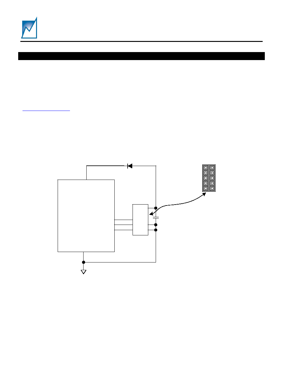
DEVELOPMENT HARDWARE & SOFTWARE
The end user can obtain the Summit SMX3200
programming system for device prototype
development. The SMX3200 system consists of a
programming Dongle, cable and Windows GUI
software. It can be ordered on the website or from a
local representative. The latest revisions of all
software and an application brief describing the
SMX3200 is available from the website
(
www.summitmicro.com
).
The SMX3200 programming Dongle/cable
interfaces directly between a PC's parallel port and the
target application. The device is then configured on-
screen via an intuitive graphical user interface
employing drop-down menus.
The Windows GUI software will generate the data
and send it in I
2
C serial bus format so that it can be
directly downloaded to the SMS64 via the
programming Dongle and cable. An example of the
connection interface is shown in Figure 2.
When design prototyping is complete, the software
can generate a HEX data file that should be
transmitted to Summit for approval. Summit will then
assign a unique customer ID to the HEX code and
program production devices before the final electrical
test operations. This will ensure proper device
operation in the end application.
Pin 9, 5V
Pin 7, 10V
Pin 5, Reserved
Pin 3, GND
Pin 1, GND
Pin 6, MR#
Pin 4, SDA
Pin 2, SCL
Pin 8, Reserved
Pin 10, Reserved
Top view of straight 0.1" x 0.1 closed-side
connector. SMX3200 interface cable connector.
9
7
5
3
1
10
8
6
4
2
SMS64
SDA
SCL
VCC_CAP
GND
0.1
F
Positive
Supply
Com m on
Ground
M R#
D1
C1
Figure 2 ≠ SMX3200 Programmer I
2
C serial bus connections to program the SMS64. Normally SDA and SCL
signals require on board pull-up resistors, however, both the SMS64 and the SMX3200 have internal pull-up
resistors. D1 is needed between the Dongle Supply and Vcc_Cap so that there will be no contention
between the two supplies. C1 is for noise bypassing.
SMS64
Preliminary
Summit Microelectronics, Inc
2060 2.22 10/09/03
10
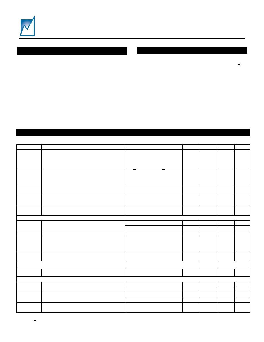
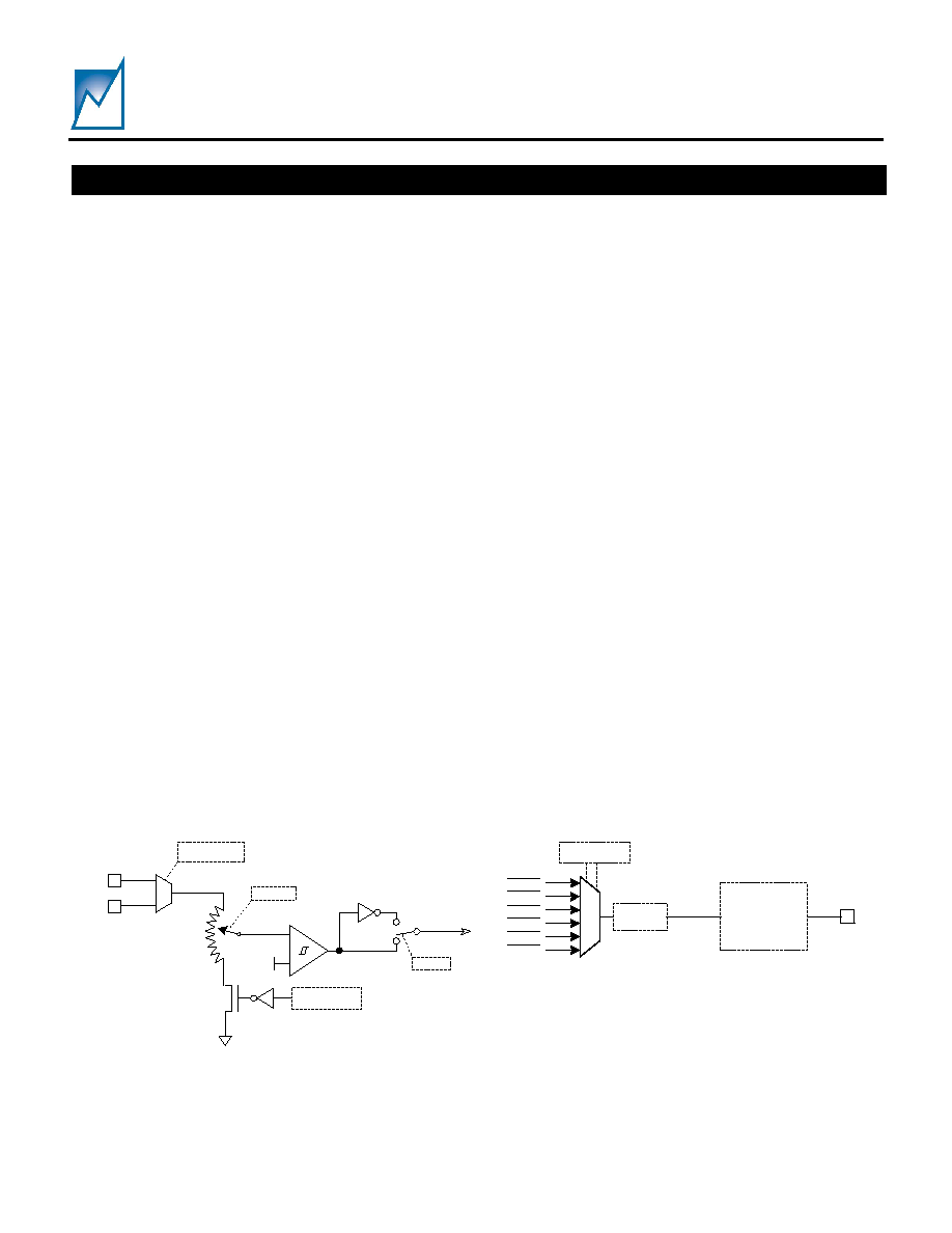
VOLTAGE MONITOR
Figure 3 shows a block diagram of a voltage
monitor. The curved resistive element is a symbolic
representation of a non-volatile DAC. When using the
SMX3200 (dongle) and GUI software the threshold
level that is selected is programmed into the SMS64,
effectively adjusting the output of the DAC to the
requested threshold detection level. The internal
detection circuit resolution is 8-bits and the threshold
detection range is 0.9V to 6.0V. This allows adjusting
the programmable threshold voltage (V
PTH
) in 20mV
increments.
In applications where the voltage to be monitored
is outside the standard range, or is even a negative
voltage, the `naked input' option can be selected. This
will effectively disconnect the DAC from ground
making the VCC and VM high impedance inputs to the
DAC. With this option selected the input is directly
compared to the internal reference voltage of 0.5V.
This will require the use of an external resistor divider
circuit. If this option is selected, the user must insure
that the external resistors will not allow the VCC or VM
inputs to exceed the recommended operating ranges.
The comparator has two mux'ed voltage inputs,
VCC and VM. The VCC inputs are used as
`precondition qualifiers' (No fault conditions exist)
before the SMS64 is ready to begin any power-on
sequence. Once the sequence has commenced the
mux will automatically switch the comparator to the
VM input. {When using the GUI for the SMS64 this
option is on the channel settings tab and located in the
block designated `triggers'}
The VCC inputs are also used as the supply input
for the SMS64. Internally all of the VCC inputs are
diode-OR'ed and the highest VCC input will effectively
become the SMS64 VDD supply. If the VCC input is
not selected as a precursor to power-on, it can be tied
to the corresponding VM input, left open or be tied to
one of the other VCC inputs
The output of the comparator is programmable to
generate either an over-voltage or under-voltage
signal.
PUP OUTPUTS
The primary function of the PUP outputs is to turn-
on or switch external power sources; for example,
turning on low drop-out regulators or DC-to-DC
converters or by providing a high-side drive output to a
MOSFET (Figure 4)
Each PUP output can be programmed as active
high or active low. If active low, the SMS64 will pull
the PUP output to GND in its active state. An external
pull-up resistor must be tied to the PUP output.
If active high is selected, an inactive PUP output
will be pulled low. Asserting the PUP output will
release the open drain output, necessitating an
external pull-up resistor. When the PUP outputs are
configured as active high or active low they must not
be pulled-up to a potential higher than VDD_CAP.
The PUP output can also be configured as a high-
side driver that can be used to turn on the gate of
an external MOSFET. The gate voltage for all PUP
outputs can be programmed to either 10.5V or 14.5V.
APPLICATIONS INFORMATION
PUP
X
Delay 'up'
Delay 'dn'
Input Select
UV/OV
C
UV/OV
A
UV/OV
B
UV/OV
F
UV/OV
D
UV/OV
E
Highside Driver
Active High
Active Low
Figure 4. PUP Configuration Diagram
-
+
V
REF
VCC
VM
NV-DAC
'naked' input
select
UV/OV
Input Select
Figure 3. Voltage Monitor Diagram

SMS64
Preliminary
Summit Microelectronics, Inc
2060 2.22 10/09/03
11
POWER SEQUENCING
The SMS64 is a programmable controller for power
supply sequencing. Up to six channels can be
sequenced in any order with several delay options.
In order for a power supply to be sequenced it must
be enabled by a PUP output and monitored by the
corresponding VM input. This channel must also be
programmed to participate in the sequence and be
assigned to a sequence position. If a channel is not
programmed to participate in the sequence it should
be assigned to the null sequence position (position 7)
and the channel will act strictly as a voltage monitor.
A sequence position is given to each channel as an
order to the sequence. The sequence position
assignments must begin at position 0 and must not
skip positions. Also, multiple channels can be
programmed into the same sequence position to
enable more than one supply at a time. Note: If two
or more channels with high voltage PUP outputs share
the same sequence position their power-on delays
must be either equal or differ by at least t
SLEW
(time it
takes for the PUP output to slew from 0V to the level
of VGG_CAP).
Each channel selected for sequencing is given a
power-on and power-off delay. The power-on delay is
a delay from the VM input of one channel going out of
fault to the PUP output of another channel going
active. The power-off delay is the delay from the VM
input of one channel turning off to the PUP output of
another channel that is turning off. The power-on and
power-off delay options are 25ms, 50ms, 100ms and
200ms. If the fast times option is selected in the
configuration register, these delays are divided by 16
(1.5625ms, 3.125ms, 6.25ms and 12.5ms).
Before the SMS64 begins the power-on
sequencing the voltage monitors are monitoring the
VCC inputs. The power-on sequencing will not begin
until all of the VCC inputs that are selected as
precursors to power-on sequencing are out of their
fault conditions, the `precondition qualifiers'.
Power-on sequencing can be initiated by toggling
the PWR_ON/OFF pin from low to high or by writing to
the power-on bit of the command register. For
automatic start-up the PWR_ON/OFF can be floated
as the device receives power. Either of these will
initiate the power-on sequence as soon as the
precursor conditions are met. During the power-on
sequence power-off commands as well as activity on
the PWR_ON/OFF pin is ignored.
The power-on sequencing begins with the power-
on delay time of the channel(s) in sequence position 0.
Once this delay has timed out the PUP will go active.
At this point the supply connected to the VM input will
begin to turn on. When this supply reaches its
programmed threshold (under-voltage) and the PUP
output has reached the level of VGG_CAP (high
voltage PUP outputs only) the sequence position
counter will change to position 1 and the power-on
delay timer for the channel(s) in sequence position 1
will begin. This will repeat until all channels that were
programmed for sequencing have turned on and are
not in fault conditions. Once sequencing is complete
RST_B# will clear after t
PRTO
.
Power-off sequencing can be initiated by a high to
low transition on the PWR_ON/OFF pin, by writing to
the power-off bit of the command register, or triggered
off of a selected fault condition. The SMS64 can be
configured to sequence the supplies off in the same
order or reverse order of the power-on sequence.
During the power-off sequence power-on commands
as well as activity on the PWR_ON/OFF pin is ignored.
The power-off sequencing begins with the power-
off delay time of the channel(s) in the last sequence
position of the power-on sequence (reverse order).
Once this delay has timed out the PUP will turn off. At
this point the supply connected to the VM input will
begin to turn off. When this supply falls below 0.8V
the sequence position counter will change to the next
position and the power-off delay timer for the
channel(s) in current sequence position will begin.
This will repeat until all channels that were
programmed for sequencing have turned off. At this
point the voltage monitors will switch from the VM
inputs to the VCC inputs to monitor for the precursor
conditions to power-on sequencing. Note: With the
OFF sensors disabled (configuration option) the
SMS64 will immediately increment to the next
sequence position instead of waiting until the VM
inputs reach 0.8V.
FORCED SHUTDOWN
The forced shutdown function is always enabled.
This function is used to immediately turn off all PUP
outputs when there is not enough time to perform a
power-off sequence. Forced shutdown can be
initiated by pulling the FS# pin low, by writing to the
forced shutdown bit of the command register, or
triggered off of a selected fault condition.
APPLICATIONS INFORMATION (CONTINUED)

SMS64
Preliminary
Summit Microelectronics, Inc
2060 2.22 10/09/03
12
The SMS64 can be configured to latch a forced
shutdown until either power is recycled to the device
or until all the VM inputs of the channels used in
sequencing have fallen below 0.8V. Note: With the
latter configuration and with the OFF sensors disabled,
the SMS64 will not latch a force shutdown command.
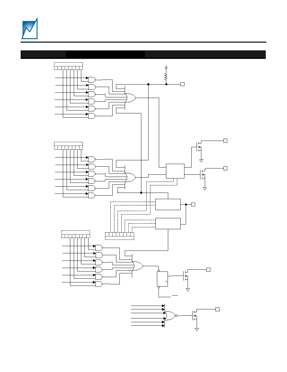
RST_A# OUTPUT
RST_A# has eight sources for activation (see
Figure 5). Any one of the voltage monitor UV/OV
outputs can be programmed as a source. If a selected
UV/OV condition occurs, the RST_A# output will be
driven low and remain low so long as the fault
condition is present. If the fault condition is cleared,
RST_A# will remain low for t
PRTO
(programmed reset
timeout period) and then return high.
If the MR# input is taken low, RST_A# will be
asserted. RST_A# will remain active so long as MR#
is low, and will continue driving the RST_A# output for
t
PRTO
after MR# returns high. The affect of the MR#
input on RSTA# cannot be bypassed or disabled.
If the Longdog timer is enabled, RST_A# will be
driven low and remain low for t
PRTO
after a Longdog
time out period.
During power-on sequencing RST_A# can be
cleared by a selected PUP output going active,
provided there are no other RST_A# triggers active
and that RST_A# has been triggered prior to this
event.. This allows RST_A# to be cleared prior to
RST_B#: thereby, providing a mechanism to bring one
portion of circuitry out of reset before another.
RST_B# OUTPUT
RST_B# has eight sources for activation (see
Figure 5). Any one of the voltage monitor UV/OV
outputs can be programmed as a source. If a selected
UV/OV condition occurs, the RST_B# output will be
driven low and remain low so long as the fault
condition is present. If the fault condition is cleared,
RST_B# will remain low for t
PRTO
and then return high.
If the MR# input is taken low, RST_B# will be
asserted. RST_B# will remain active so long as MR#
is low, and will continue driving the RST_B# output for
t
PRTO
after MR# returns high. The affect of the MR#
input on RSTB# cannot be bypassed or disabled.
If the Longdog timer is enabled, RST_B# will be
driven low and remain low for t
PRTO
after a Longdog
time out period.
IRQ# OUTPUT
The IRQ# circuitry is disabled during power-on
sequencing until all reset have cleared and the reset
interval (t
PRTO
) has timed out. This allows the
application circuit to become fully operational before
an interrupt can occur. Interrupts are also disabled
during power-off sequencing and whenever the FS#
input is asserted.
IRQ# has seven sources of activation (see Figure
5). Any one of the voltage monitor UV/OV outputs can
be programmed as a source. If a selected UV/OV
condition occurs, the IRQ# output will be driven low
and remain low so long as the fault condition is
present.
The IRQ# output will be asserted if the Watchdog
timer times out. The Watchdog timer can be bypassed
by programming it off.
After the UV/OV condition has cleared or after the
Watchdog timer times out, the IRQ# output can be
cleared by two events. If either RST_A# or RST_B#
times out and returns high, the IRQ# output will be
cleared. The IRQ# output will also be cleared by a low
to high transition on the WLDI input. IRQ# can be
cleared under software control by writing 10
[HEX]
to the
command register.
HEALTHY# OUTPUT
The HEALTHY# output reflects the state of all of
the VM inputs (see Figure 5). The HEALTHY# output
will be driven low if there are no fault conditions
present.
APPLICATIONS INFORMATION (CONTINUED)
SMS64
Preliminary
Summit Microelectronics, Inc
2060 2.22 10/09/03
13
APPLICATIONS INFORMATION (CONTINUED)
TIMER REG
LONGDOG
TIM ER
W LDI
M R#
RESET
TIM ER
RST_A#
RST_B#
UV/OV
C
UV/OV
A
UV/OV
B
UV/OV
D
UV/OV
E
RSTA Enable Reg
UV/OV
F
UV/OV
C
UV/OV
A
UV/OV
B
UV/OV
D
UV/OV
E
RSTB Enable Reg
UV/OV
F
W ATCHDOG
TIM ER
UV/OV
C
UV/OV
A
UV/OV
B
UV/OV
D
UV/OV
E
IRQ Enable Reg
UV/OV
F
W LDI
IRQ#
SET
CLR
Q
Q
HEALTHY#
UV/OV
C
UV/OV
A
UV/OV
B
UV/OV
D
UV/OV
E
UV/OV
F
VDD
Figure 5. Reset and Interrupt Generation Block Diagram
SMS64
Preliminary
Summit Microelectronics, Inc
2060 2.22 10/09/03
14
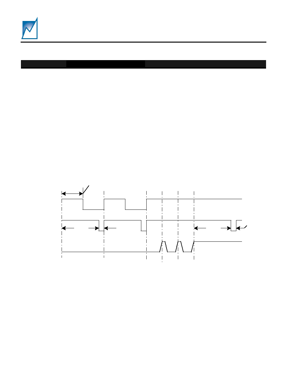
WATCHDOG AND LONGDOG TIMERS
The SMS64 contains two timers that can be
programmed independently. The Watchdog timer will
generate an interrupt if it times out. The Longdog timer
will generally be programmed to be of longer duration
than the Watchdog timer and will generate a reset if it
times out. Both timers are cleared by a low to high
transition on WLDI and start simultaneously.
If the Longdog times out RST_A# and RST_B# will
be driven low either until a WLDI clear is received or
until t
PRTO
(whichever occurs first), at which time they
will return high. When RST_A# and RST_B# return
high both timers are reset to time zero. Therefore, if
the Longdog t
PLDTO
is shorter than the Watchdog
t
PWDTO
, RST_A# and RST_B# will effectively clear the
interrupt before it can drive the output low
If WLDI is held low the timers will free-run
generating a series of interrupts and resets. If WLDI is
held high the interrupt (Watchdog) output will be
disabled and only the reset (Longdog) outputs will be
active.
Refer to Figure 6 which illustrates the action of
RST_A#, RST_B# and IRQ# with respect to the
Watchdog and Longdog timers and the WLDI input.
t
PRTO
t
PLDTO
t0
t0
t
PWDTO
t0
t0
t0
t0
t
PLDTO
t
PRTO
RST_A#
RST_B#
IRQ#
WLDI
Figure 6. Watchdog, Longdog and WLDI Timing Diagram
APPLICATIONS INFORMATION (CONTINUED)
SMS64
Preliminary
Summit Microelectronics, Inc
2060 2.22 10/09/03
15
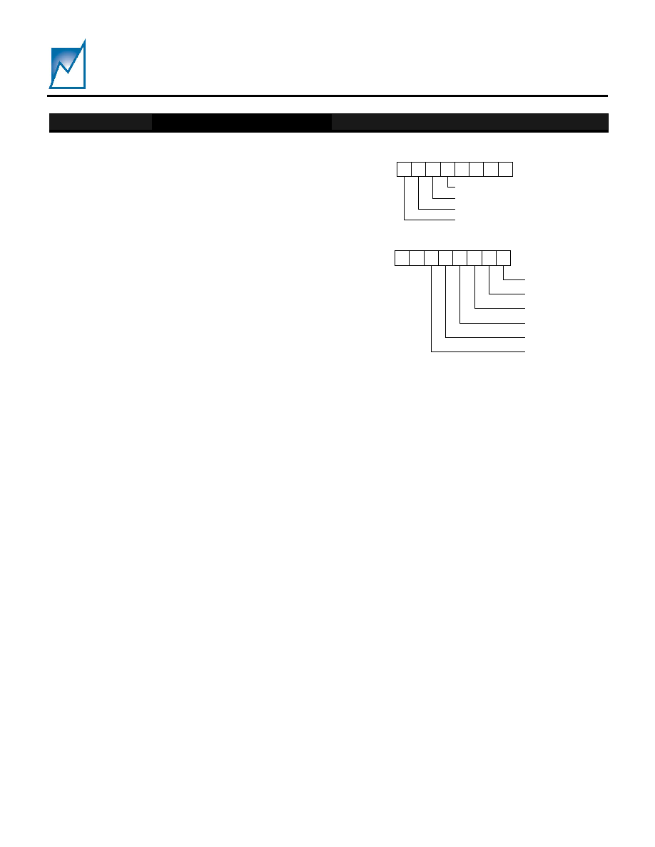
COMMAND REGISTER
The command register (slave address 1001
[BIN]
register address 0F
[HEX]
) contains 4 bits used for
software control of several functions in the SMS64
(see Figure 7). Each of these functions is activated by
writing a 1 to the function's bit in the command register
(listed below). Only one command can be issued at a
time; therefore, only data bytes 80
[HEX]
, 40
[HEX]
, 20
[HEX]
,
10
[HEX]
and 00
[HEX]
should be written to the command
register. The command register is volatile and will be
cleared when power is removed.
Bit 7 is the power-on bit. When active it will initiate a
power-on sequence.
Bit 6 is the power-off bit. When active it will initiate a
power-off sequence.
Bit 5 is OR'ed with the FS# pin. When active it will
turn off all PUP outputs.
Bit 4 is OR'ed with the WLDI pin. When active it will
clear both the Longdog and Watchdog timers and
block interrupts.
FAULT and STATUS REGISTERS
The fault and status registers (see Figure 7) are
volatile registers which reflect the conditions of the VM
inputs. In either register a fault condition (under-
voltage or over-voltage) is represented as a "1".
The Fault register (located at register address 0D
[HEX]
) latches the state of the VM inputs when an IRQ#
is generated.
The Status register (located at register address 0E
[HEX]
) reflects the current state of the VM inputs.
CONFIGURATION REGISTERS
The SMS64 has 24 configuration registers that
allow programming voltage thresholds, timer values,
sequencing order and output configurations. All of
these registers are accessible over the I
2
C serial
interface.
For prototyping purposes, Summit can provide a
programming cable (SMX3200) that interfaces a PC
parallel port to the serial interface of the SMS64 (see
the `Development Hardware and Software' section).
Summit provides software that can be downloaded
from its website without charge. The software
provides an intuitive graphical user interface
comprised of drop-down menus that make selecting
options straightforward, thereby eliminating the need
to understand the register configurations in detail.
MEMORY ARRAY
The SMS64 has 4-K bits of nonvolatile memory
that is accessible over the 2-wire serial interface. This
memory can be used in a dynamic manner by the host
processor or it could be used to store board
configuration information or board identification
information. The slave address used to access the
memory can be configured as 1010
[BIN]
or 1011
[BIN].
The memory array can be read whenever chip
select is enabled (CS# low). In order to prevent
inadvertent writes, memory writes are blocked when
either RST_A# or RST_B# are active. Therefore, the
memory can only be written after the device has
performed a power-on operation, the reset outputs
(RST_A# and RST_B#) have timed out and before the
device has been issued a force shutdown or power-off
command. MR# must also be high.
7
6
5
4
3
2
1
0
Command Register
1 = FS
1 = PWR_DOWN
1 = PWR_UP
1 = WLDI
UV/OV
A
UV/OV
B
UV/OV
C
UV/OV
D
UV/OV
E
UV/OV
F
5
4
3
2
1
0
Fault & Status Register
Figure 7 ≠ Command and Status Registers
APPLICATIONS INFORMATION (CONTINUED)
SMS64
Preliminary
Summit Microelectronics, Inc
2060 2.22 10/09/03
16
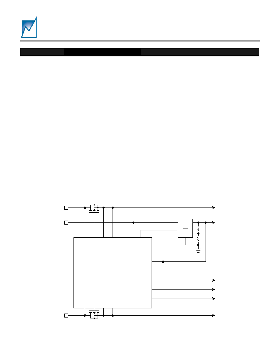
Applications Example
A simple application example is shown in Figure 8.
Three voltages are provided by a motherboard, +5V,
+3.3V, and +1.8V. The +5V and +3.3V supplies are
switched on through series MOSFETS and applied to
the application circuit. The +1.8V supply will drive an
LDO, supplying +1.2V to the application circuit. The
application requires that the power supplies sequence
in the following order: +1.2V, +3.3V, +5.0V. As these
supplies are sequenced on, RST_A# is cleared after
the +1.2V supply has reached its under-voltage
threshold. RST_B# is not cleared until the +3.3V and
+5.0V supplies have reached their under-voltage
threshold. After the supplies have sequenced on, a
10% under-voltage on the +1.2V supply will trigger
RSTA#. Similarly, a 10% under-voltage on the +3.3V
supply will trigger RSTB#. The devices driven by the
application circuit require that if a 10% under-voltage
occurs on the +5.0V supply, the SMS64 will generate
an IRQ#. A 10% over-voltage on any supply will
trigger both RSTA# and RSTB#. This application also
requires that the power supplies are sequenced off in
the reverse order that they were sequenced on. The
power supply sequencing is controlled by toggling the
PWR_ON/OFF pin. With these requirements, the
SMS64 is configured as follows:
Channel A
Sequenced; Sequence Position 2; Power-On
Delay(t
DPONA
) = 50ms; Power-Off Delay(t
DPOFFA
) =
50ms;
Under-voltage; Programmable Threshold(V
PTHA
) =
4.50V
Channel B
Sequenced; Sequence Position 1; Power-On
Delay(t
DPONB
) = 25ms; Power-Off Delay(t
DPOFFB
) =
25ms;
Under-voltage; Programmable Threshold(V
PTHB
) =
2.96V
Channel C
Sequenced; Sequence Position 0; Power-On
Delay(t
DPONC
) = 50ms; Power-Off Delay(t
DPOFFC
) =
100ms;
Under-voltage; Programmable Threshold(V
PTHC
) =
1.06V
Channel D
Not Sequenced; Sequence Position null (7);
Over-voltage; Programmable Threshold(V
PTHD
) =
5.50V
+5.0V
SMS64
+3.3V
VCC
A
PU
P
A
VM
A
VM
C
VM
D
VC
C
B
PU
P
B
VM
B
VM
E
VM
F
PU
P
C
VCC
C
IRQ#
RSTA#
RSTB#
GND
V+
OUT
SET
ON/OFF
+1.8V
+1.2V
+5.0V
+3.3V
Figure 8 ≠ Simple Applications Example
APPLICATIONS INFORMATION (CONTINUED)
SMS64
Preliminary
Summit Microelectronics, Inc
2060 2.22 10/09/03
17
Channel E
Not Sequenced; Sequence Position null (7);
Over-voltage; Programmable Threshold(V
PTHE
) =
3.64V
Channel F
Not Sequenced; Sequence Position null (7);
Over-voltage; Programmable Threshold(V
PTHF
) =
1.34V
Power-Off in reverse order
RST_A# triggered by channels C, D, E, and F; cleared
on PUPB active
RST_B# triggered by channels B, D, E, and F
IRQ# triggered by channel A
VCCA, VCCB, and VCCC selected as precursors to
power-on sequencing
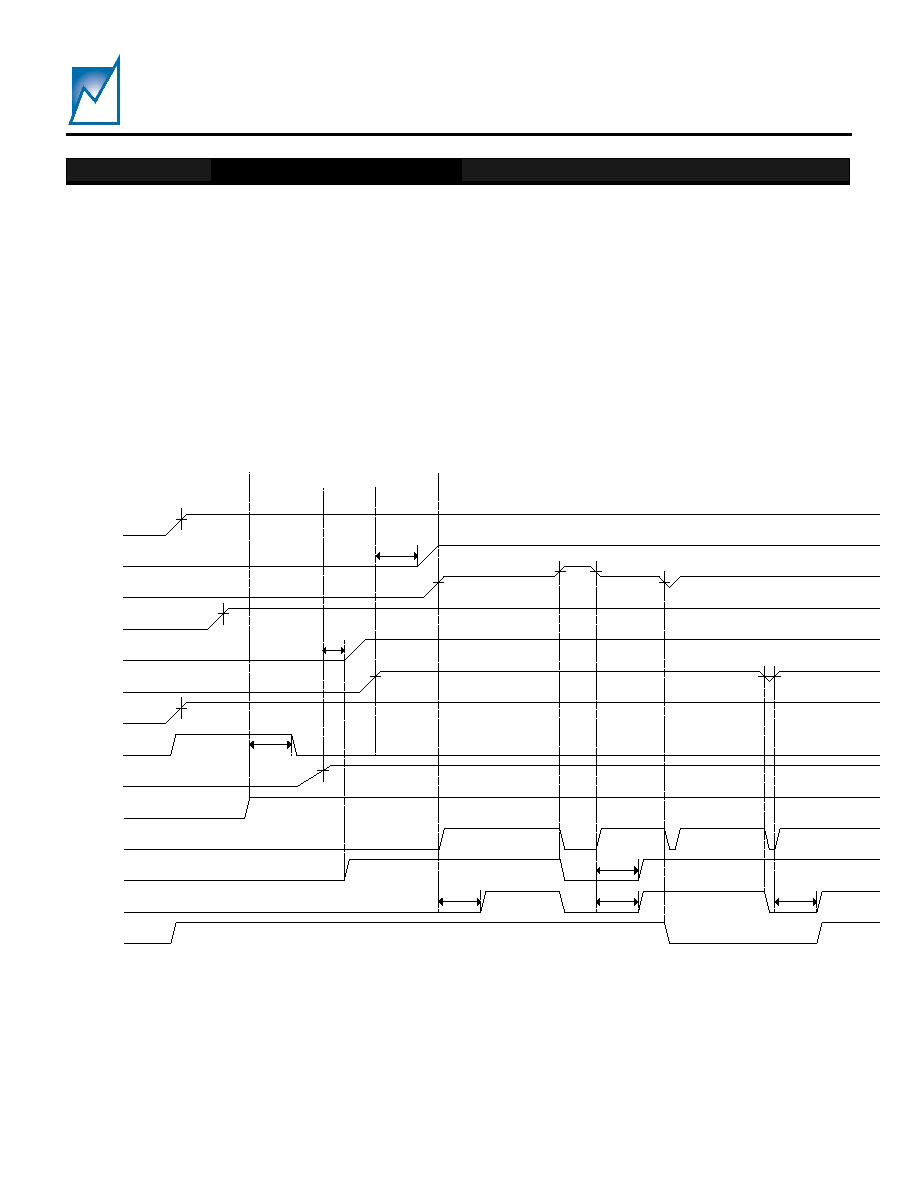
The resulting timing diagram is shown in Figures 9
and 10. Figure 9 shows the SMS64 sequencing the
supplies on and then monitoring for fault conditions.
Figure 10 shows the SMS64 sequencing the supplies
off then sequencing the supplies on.
VM
B,E
VCC
A
VCC
B
PUP
A
VM
A,D
PUP
B
VM
C,F
PUP
C
RST_A#
RST_B#
IRQ#
HEALTHY#
PWR_ON/OFF
V
PTHA
Sequence
Position 0
Sequence
Position 1
Sequence
Position 2
t
DPONB
t
PRTO
t
PRTO
t
PRTO
V
PTHB
V
PTHB
V
PTHD
V
PTHD
V
PTHB
Power-On
VCC
C
V
PTHC
t
DPONC
V
PTHC
t
DPONA
V
PTHA
V
PTHA
t
PRTO
Figure 9 - The SMS64 sequencing the supplies on and then monitoring for fault conditions.
APPLICATIONS INFORMATION (CONTINUED)
SMS64
Preliminary
Summit Microelectronics, Inc
2060 2.22 10/09/03
18
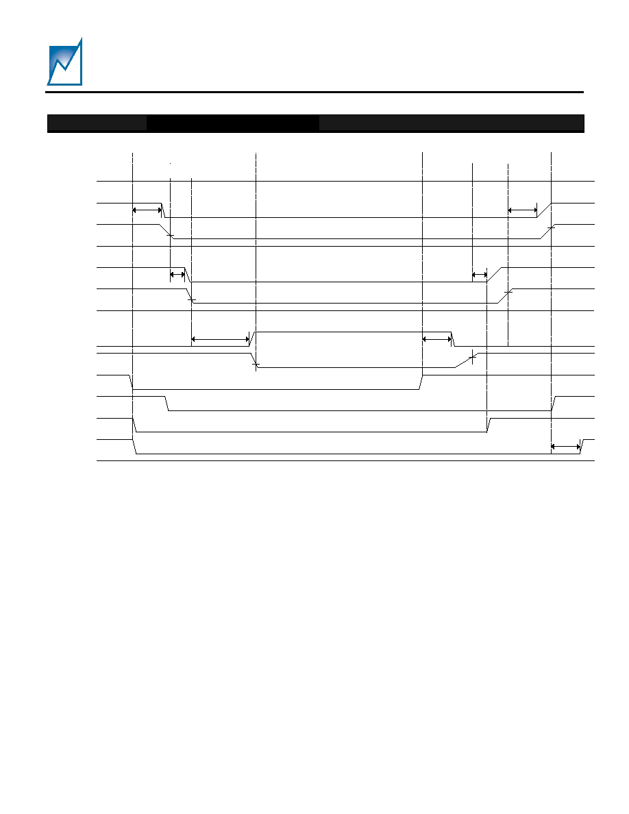
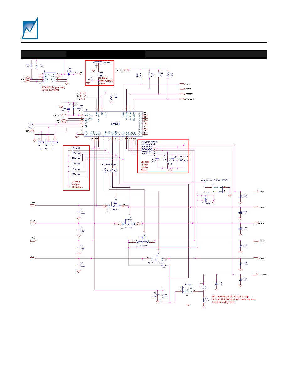
Additional Considerations
An example application circuit is shown in Figure
11. Additional optional noise bypassing components
are shown for the VMX monitor pins. These
components consist of ferrite bead inductors and
capacitors. They may be necessary in very noisy
systems where tight undervoltage/overvoltage
tolerances are needed.
The PUP output pins require series resistors to drive
the gates of the power mosfets. Gate capacitors (C27
thru C32) are also recommended to prevent initial
mosfet, LDO or dc-dc converter turn-on during the
SMS64 power on sequence. To minimize transient
power surges in hot-swappable line card designs,
place a 0.01
µF (10nF), 25V, ceramic capacitor on
each PUP output pin to ground.
The PUP output level is programmable to either
logic-level, 10.5V or 14V depending on the type of
power component used in the system. To minimize
the voltage drop across the power mosfets, the device
needs to be fully enhanced to minimize RDS
(ON)
.
However, some mosfets have maximum VGS
specifications of 15V while others are 20V. For
improved sequencing performance with the SMS64, it
is recommended to use the lower rated VGS devices
with the PUP outputs set to 10.5V instead of 14V. The
industry trend for power mosfets is toward lower VGS
specs while also maintaining low RDS
(ON)
specifications.
VM
B,E
VCC
A
VCC
B
PUP
A
VM
A,D
PUP
B
VM
C,F
PUP
C
RST_A#
RST_B#
IRQ#
HEALTHY#
PW R_ON/OFF
Sequence
Position 0
Sequence
Position 1
Sequence
Position 2
t
PRTO
Sequence
Position 0
Sequence
Position 1
Sequence
Position 2
t
DPOFFB
t
DPOFFC
V
OFF
V
OFF
V
OFF
Power-Off
Power-On
t
DPOFFA
VCC
C
t
DPONB
V
PTHB
t
DPONC
V
PTHC
t
DPONA
V
PTHA
Figure 10 - The SMS64 sequencing the supplies off then sequencing the supplies back on.
APPLICATIONS INFORMATION (CONTINUED)
SMS64
Preliminary
Summit Microelectronics, Inc
2060 2.22 10/09/03
19
Figure 11 ≠ Example Applications Schematic. In this example, the SMS64 sequences six individual output
supply voltages derived from four separate input power supplies by turning on 4 power mosfet switches, one
LDO and one dc-dc converter. Six individual input supplies could also be sequenced if needed. The SMS64
can sequence mosfets switches or any other power source with either a negative or positive enable inputs.
APPLICATIONS INFORMATION (CONTINUED)
SMS64
Preliminary
Summit Microelectronics, Inc
2060 2.22 10/09/03
20
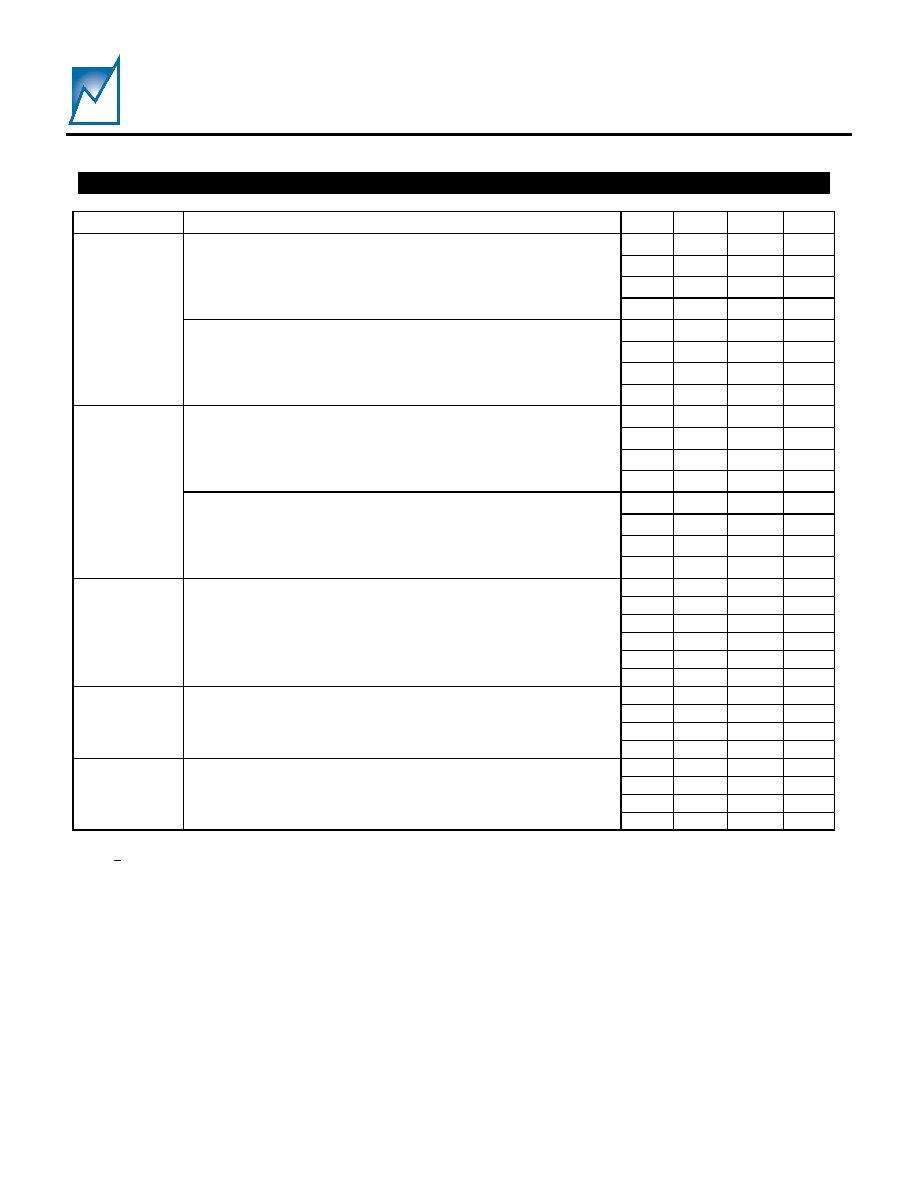
DEFAULT CONFIGURATION REGISTER SETTINGS ≠ SMS64F-116
Register
Hex Contents
Configured as:
R00
B9
Channel A UV Trip Point = 4.6V
R01
69
Channel B UV Trip Point = 3.0V
R02
37
Channel C UV Trip Point = 2.0V
R03
19
Channel D UV Trip Point = 1.4V
R04
05
Channel E UV Trip Point = 1.0V
R05
05
Channel F UV Trip Point = 1.0V
R06
80
Use Channel A In Sequencing [D7]
VCCX To PUPA On Delay = 200ms [D6:5]
VCCX To PUPA Off Delay = 200ms [D4:3]
PUPA Sequence Position set to 0 [D2:0]
R07
81
Use Channel B In Sequencing [D7]
VCCX To PUPB On Delay = 200ms [D6:5]
VCCX To PUPB Off Delay = 200ms [D4:3]
PUPB Sequence Position set to 1 [D2:0]
R08
82
Use Channel C In Sequencing [D7]
VCCX To PUPC On Delay = 200ms [D6:5]
VCCX To PUPC Off Delay = 200ms [D4:3]
PUPC Sequence Position set to 2 [D2:0]
R09
83
Use Channel D In Sequencing [D7]
VCCX To PUPD On Delay = 200ms [D6:5]
VCCX To PUPD Off Delay = 200ms [D4:3]
PUPD Sequence Position set to 3 [D2:0]
R0A
84
Use Channel E In Sequencing [D7]
VCCX To PUPE On Delay = 200ms [D6:5]
VCCX To PUPE Off Delay = 200ms [D4:3]
PUPE Sequence Position set to 4 [D2:0]
R0B
85
Use Channel F In Sequencing [D7]
VCCX To PUPF On Delay = 200ms [D6:5]
VCCX To PUPF Off Delay = 200ms [D4:3]
PUPF Sequence Position set to 5 [D2:0]
R0C
00
PUP On/Off Use fast times set to OFF [D7]
Longdog Timer set to Off [D6:5]
RST Timeout Interval set to 25ms [D4:3]
Watchdog Timer set to Off [D2:0]
SMS64
Preliminary
Summit Microelectronics, Inc
2060 2.22 10/09/03
21
DEFAULT CONFIGURATION REGISTER SETTINGS ≠ SMS64F-116 (Cont.)
R10
47
RSTA Trigger on VA Over/UnderVoltage set to RST On VA UV/OV [D0]
RSTA on VB Over/UnderVoltage set to RST On VB UV/OV [D1]
RSTA on VC Over/UnderVoltage set to RST On VC UV/OV [D2]
RSTA on VD Over/UnderVoltage set to No Reset [D3]
RSTA on VE Over/UnderVoltage set to No Reset [D4]
RSTA on VF Over/UnderVoltage set to No Reset [D5]
Memory (EE) Slave Address set to 1010 [D7]
R11
38
RSTB on VA Over/UnderVoltage set to No Reset [D0]
RSTB on VB Over/UnderVoltage set to No Reset [D1]
RSTB on VC Over/UnderVoltage set to No Reset [D2]
RSTB on VD Over/UnderVoltage set to RST On VD UV/OV [D3]
RSTB on VE Over/UnderVoltage set to RST On VE UV/OV [D4]
RSTB on VF Over/UnderVoltage set to RST On VF UV/OV [D5]
R12
00
IRQ on VA Over/UnderVoltage set to No IRQ [D0]
IRQ on VB Over/UnderVoltage set to No IRQ [D1]
IRQ on VC Over/UnderVoltage set to No IRQ [D2]
IRQ on VD Over/UnderVoltage set to No IRQ [D3]
IRQ on VE Over/UnderVoltage set to No IRQ [D4]
IRQ on VF Over/UnderVoltage set to No IRQ [D5]
R13
00
PowerOff on VA Over/UnderVoltage set to No PowerOff [D0]
PowerOff on VB Over/UnderVoltage set to No PowerOff [D1]
PowerOff on VC Over/UnderVoltage set to No PowerOff [D2]
PowerOff on VD Over/UnderVoltage set to No PowerOff [D3]
PowerOff on VE Over/UnderVoltage set to No PowerOff [D4]
PowerOff on VF Over/UnderVoltage set to No PowerOff [D5]
R14
3F
Use Naked Input VA set to No [D0]
Use Naked Input VB set to No [D1]
Use Naked Input VC set to No [D2]
Use Naked Input VD set to No [D3]
Use Naked Input VE set to No [D4]
Use Naked Input VF set to No [D5]
R15
3F
VA Over/Undervoltage set to Under [D0]
VB Over/Undervoltage set to Under [D1]
VC Over/Undervoltage set to Under [D2]
VD Over/Undervoltage set to Under [D3]
VE Over/Undervoltage set to Under [D4]
VF Over/Undervoltage set to Under [D5]
SMS64
Preliminary
Summit Microelectronics, Inc
2060 2.22 10/09/03
22
DEFAULT CONFIGURATION REGISTER SETTINGS ≠ SMS64F-116 (Cont.)
R16
3F
PUPA High/Low Logic Level set to High [D0]
PUPB High/Low Logic Level set to High [D1]
PUPC High/Low Logic Level set to High [D2]
PUPD High/Low Logic Level set to High [D3]
PUPE High/Low Logic Level set to High [D4]
PUPF High/Low Logic Level set to High [D5]
R17
0F
PUPA High Voltage/Logic Level set to HV [D0]
PUPB High Voltage/Logic Level set to HV [D1]
PUPC High Voltage/Logic Level set to HV [D2]
PUPD High Voltage/Logic Level set to HV [D3]
PUPE High Voltage/Logic Level set to not HV [D4]
PUPF High Voltage/Logic Level set to not HV [D5]
R18
08
RSTA Cleared on PUPA Active set to No [D0]
RSTA Cleared on PUPB Active set to No [D1]
RSTA Cleared on PUPC Active set to No [D2]
RSTA Cleared on PUPD Active set to Yes [D3]
RSTA Cleared on PUPE Active set to No [D4]
RSTA Cleared on PUPF Active set to No [D5]
R19
01
Vgate Select set to 14.5V [D0]
No ACK For Slave Address 1001 set to ACK [D1]
Configuration Lock Option set to Unlocked [D2]
Force Shutdown Instead Of Cascade Down set to No [D3]
Force Shutdown Latched Until POR set to No [D4]
Forward Or Reverse PUP Order set to Reverse [D5]
Memory (EE) Slave Address set to 1010 [D7]
R1D
0F
Ready After VCCA OK set to Ready [D0]
Ready After VCCB OK set to Ready [D1]
Ready After VCCC OK set to Ready [D2]
Ready After VCCD OK set to Ready [D3]
Ready After VCCE OK set to Not Used [D4]
Ready After VCCF OK set to Not Used [D5]
Application Note 32 contains a complete description of the Windows GUI and the default
settings of each of the 24 individual Configuration Registers.
SMS64
Preliminary
Summit Microelectronics, Inc
2060 2.22 10/09/03
23
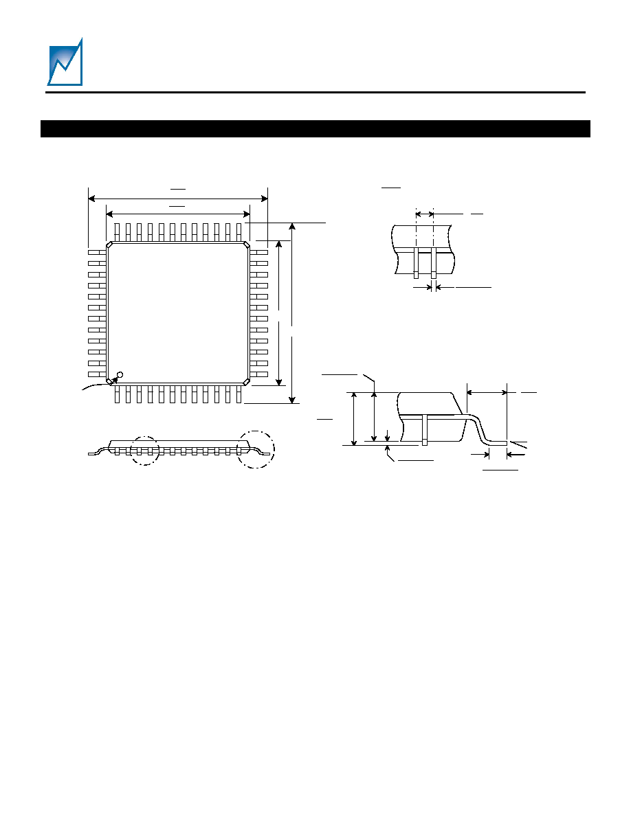
PACKAGES
A
B
Pin 1
Indicator
Inches
(Millimeters)
0.002 - 0.006
(0.05-0.15)
MAX.
0.047
(1.2)
0.037 - 0.041
0.95 - 1.05
0.018 - 0.030
(0.45 - 0.75)
0.039
(1.00)
0.02
(0.5)
BSC
0.007 - 0.011
(0.17 - 0.27)
DETAIL "A"
DETAIL "B"
(B)
(A)
(A)
0.354
(9.00) BSC
0.276
(7.00)
BSC (B)
48 PIN TQFP PACKAGE
0
o
Min to
7
o
Max
Ref Jedec M S-026
Ref
SMS64
Preliminary
Summit Microelectronics, Inc
2060 2.22 10/09/03
24
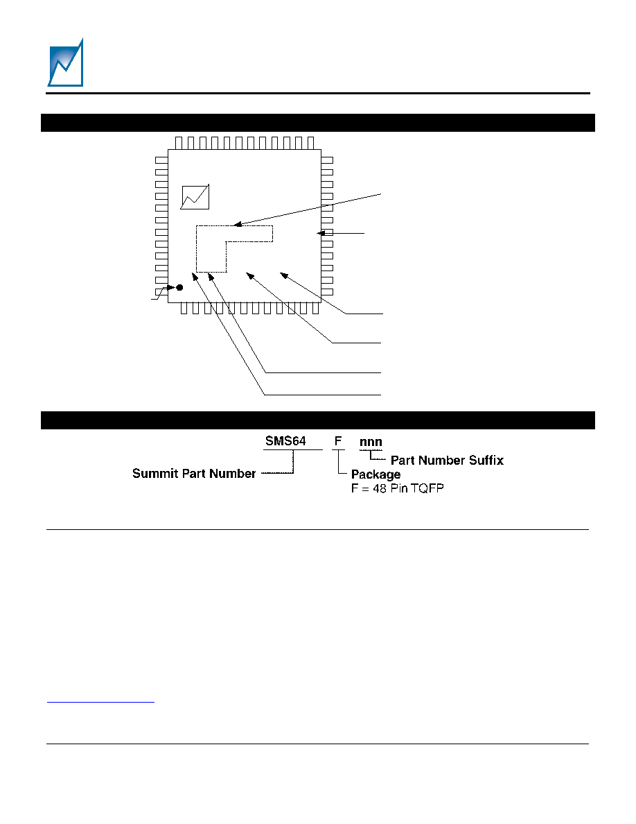
PART MARKING
SUMMIT
SMS64F
AYYWW
Pin 1
Annn
Summit Part Number
Date Code (YYWW )
Part Number suffix
Product Tracking Code
(Summit use)
Lot tracking code (Summit use)
Drawing not to scale
xx
Status Tracking Code
(Blank, MS, ES, 01, 02,...)
(Summit Use)
ORDERING INFORMATION
NOTICE
NOTE 1 - This is a Preliminary Information data sheet that describes a Summit product currently in pre-production with limited characterization.
SUMMIT Microelectronics, Inc. reserves the right to make changes to the products contained in this publication in order to improve design,
performance or reliability. SUMMIT Microelectronics, Inc. assumes no responsibility for the use of any circuits described herein, conveys no license
under any patent or other right, and makes no representation that the circuits are free of patent infringement. Charts and schedules contained
herein reflect representative operating parameters, and may vary depending upon a user's specific application. While the information in this
publication has been carefully checked, SUMMIT Microelectronics, Inc. shall not be liable for any damages arising as a result of any error or
omission.
SUMMIT Microelectronics, Inc. does not recommend the use of any of its products in life support or aviation applications where the failure or
malfunction of the product can reasonably be expected to cause any failure of either system or to significantly affect their safety or effectiveness.
Products are not authorized for use in such applications unless SUMMIT Microelectronics, Inc. receives written assurances, to its satisfaction, that:
(a) the risk of injury or damage has been minimized; (b) the user assumes all such risks; and (c) potential liability of SUMMIT Microelectronics, Inc.
is adequately protected under the circumstances.
Revision 2.22 - This document supersedes all previous versions. Please check the Summit Microelectronics Inc. web site at
www.summitmicro.com
for data sheet updates.
© Copyright 2003 SUMMIT MICROELECTRONICS, Inc.
Power Management for CommunicationsTM
I2C is a trademark of Philips Corporation.