 | –≠–ª–µ–∫—Ç—Ä–æ–Ω–Ω—ã–π –∫–æ–º–ø–æ–Ω–µ–Ω—Ç: HV111K4 | –°–∫–∞—á–∞—Ç—å:  PDF PDF  ZIP ZIP |
Inrush Limiter/Circuit Breaker/Hotswap Controller IC
HV111
Initial Release
(No External Parts Required)
Features
No External Parts Required
On Board 80V, 2A MOSFET
No Rsense Needed
±
8.0V to
±
80V Input Voltage Range
Two Level Current Limiting
1.2A Initial Inrush Limit
2.0A Second Inrush Limit/Circuit Breaker Triggers
Servo Limit to 1.2A for T
oc
then shuts down
Fast Response Current Limit when Over Current or Step
Voltage at Input Supply (eg. Diode `OR'ing)
UVLO/ENABLE & POR Supervisory Circuits
Programmable
UVLO
Over Current Protection
9.0sec Auto Retry
Built in Thermal Shutdown with Hysteresis
80V Open Drain PWRGD bar Flag
Thermally Rugged DPAK5 Package
Applications
Power Ethernet Systems
Routers, Switches
Chargers
Security Peripherals & Cameras
Automotive
Protection
Negative Supply Rail Breaking Applications
Networking Line Cards
Telecom
Line
Cards
Description
The HV111 is a complete power management solution for
switched or pluggable backplane applications up to 1.65A,
running from ≠8.0 to -80V, requiring no external components
or programming in many applications. The HV111 is not
limited to only negative input voltages. It can also be
used in +8.0 to +80V systems.
An internally programmed supervisor UVLO/ ENABLE may
be overridden with external resistors for custom settings.
Satisfying this supervisor will begin a POR phase to ensure
de-bouncing. Thereafter, a servo loop controls an internal
80V, 2A pass element to limit current. The circuit uses
internal mirrors to measure current, eliminating the need for
a sense resistor.
The HV111 includes two current modes: i) initial current limit
mode limits the current to 1.2A during turn on; ii) thereafter a
2A monitor circuit will re-trigger the servo mechanism back
to 1.2A limit if it is tripped. An on-board thermal supervisor
ensures that the device can never be damaged by over
current conditions.
Circuit breaker functionality is obtained through a either a
current limit timeout or a PWM current limiter for severe
faults. If the servo limits for more than 75ms then the part
will shut down the pass element, and initiate a 9sec timer
after which the turn on sequence will restart.
The HV111 is available in a thermally rugged DPAK-5
package which provides improved thermal resistance when
compared to SO-8 based solutions.
Typical Schematics and Waveforms
INRUSH
PWRGD
DRAIN
GND*
*Referred to ≠48V
*
*
Supertex Inc. does not recommend the use of its products in life support applications and will not knowingly sell its products for use in such applications unless it receives an adequate
"products liability indemnification insurance agreement." Supertex does not assume responsibility for use of devices described and limits its liability to the replacement of devices determined
to be defective due to workmanship. No responsibility is assumed for possible omissions or inaccuracies. Circuitry and specifications are subject to change without notice. For the latest
product specifications, refer to the Supertex website: http://www.supertex.com. For complete liability information on all Supertex products, refer to the most current databook or to the
Legal/Disclaimer page on the Supertex website.
7/24/03

HV111
Ordering Information
Package Options
DEVICE
DPAK-5
HV111 HV111K4
A
bsolute Maximum Ratings
Supply Voltage*, V
pp
-0.5V to 90V
Operating Temperature Range
-40∞C to +85∞C
Storage Temperature Range
-65∞ to +150∞C
5 Pin DPAK Thermal Resistance R
JA
80∞C/W
5 Pin DPAK Thermal Resistance R
JC
11∞C/W
* Relative to V
NN
(1) Shorted-circuit timer starts after POR timer. If V
DS
drops more than º(V
PP
-V
NN
) after t
SC
then a shorted-circuit condition exists.
Electrical Characteristics
( * means -20
∞
C< T
A
<
+85
∞
C)
Symbol Parameter
Min
Typ
Max
Units
T
A
Conditions
V
PP
Supply Voltage
-80
-8.0
V
*
V
PP
≠ V
NN
I
PP
Supply Current
1
mA
V
NN
= -48V, Standby Mode
V
UVLO
Internal UVLO Threshold (High to
Low ie. Turning Off)
-23.5 -26.0 -28.5 V *
Subtract
V
HYS
for Low-to-High
V
HYS
Internal UVLO Hysteresis
1.5
2.5
3.5
V
*
V
UV
UVLO Comparator Threshold
1.10 1.20 1.30 V * Referenced
to
V
NN
V
UVHYS
UVLO Comparator Hysteresis
60
100
140
mV
*
R
UVLO
UVLO Input Resistance
78
111
144
k
R
DS
MOSFET On Resistance
1
1.5
*
I
LEAK
Output Leakage Current
10
µ
A
*
MOSFET is off
I
INRUSH
Inrush Current Limit
1.15
1.40
1.65
A
*
I
CB
Circuit Breaker Trip Current 1.65
2.00
2.35
*
Trips then limits to I
LIMIT
until toc
expires.
I
LIMIT
Over Load Current Limiting
1.2
A
*
I
SC
Shorted Circuit PWM Average
Current
230 mA
V
PP
-V
DRAIN
< ~1V
VOL
PWRGD
PWRGD Output Low Voltage
0.4
V
I=1mA; Reference to V
NN
IOH
PWRGD
PWRGD Output leakage Current
10
µ
A
*
V=5V; Reference to V
NN
t
SC
Shorted-Circuit Timer (1) (4)
40
75
110
ms
*
t
OC
Over-Current Timer (2) (4)
40
75
110
ms
*
t
LIMIT
Current Limit Delay Time (3)
10
µ
s
*
Limits within 10
µ
s. May take
up to 100
µ
s to reach final level.
t
POR
POR Timer
2.5
4.5
6.5
ms
*
t
RESTART
Restart Timer (4)
9
Sec
*
T
OVER
Over Temperature Trip Point
120
135
150
∞
C
*
Low to High
T
RESET
Temperature Reset
70
100
∞
C
*
High to Low
(2) If the output current is in an overload condition then the output immediately goes to current limit and starts the over-current timer. If I
OUT
does not drop back
below I
LIMIT
before the timer expires then an over current condition exists. The timer is immediately reset when a fault is cleared.
(3) Time for fast return to limit circuit to react.
(4) Guaranteed by design.
2

HV111
3
Pin Description
HV111
Regulator
UVLO
POR Timer
Restart
TImer
CONTROL
LOGIC
Temperature
Sense
M1
M2
1
2000
M0
D
S
DRAIN
PWRGD
V
NN
V
PP
UVLO/
Enable
V
PP
≠
Positive voltage supply input
V
NN
≠ Negative voltage power supply input
DRAIN ≠ Internal N-Channel MOSFET drain output
UVLO/ENABLE ≠ Under Voltage lockout input or Enable
PWRGD ≠ Active Low Power Good Output
Functional Description
Many systems include front end capacitance to provide low
impedance energy and filtering to power systems. These
systems include hot pluggable live-backplane systems, such
as ≠48V telecom systems and switched systems such as
battery connected backed-up loads.
This filter capacitance, usually implemented as large
electrolytic capacitors, looks like a low impedance
connected directly across the power supply terminals and
causes high inrush currents which could damage
connectors, traces or components (such as the capacitors
themselves). These high currents may also cause localized
glitching of the backplane or EMI that could reset or interrupt
surrounding circuit cards.
The HV111 is a single chip solution that provides bullet-
proof power management control for systems with loads
less than 1.65A. See Thermal Shutdown section for power
dissipation limitation. The HV111 does not require the use of
any external components or programming and eliminates
the need for a sense resistor. Where desired, however,
internal set points may be overridden with external
components ≠ for example an external resistor divider may
be used to set the UVLO/ENABLE threshold.
High Voltage Regulator
The HV111 includes a high voltage regulator capable of
operation with V
PP
-V
NN
=8.0V to 80V. The regulator provides
an internal voltage to operate circuitry and drive the internal
1
MOSFET pass element.
Turn on Protection
(UVLO/POR for Debounce + PWM limit)
V
PP
UVL
O/
ENABLE
PWRGD
DRAIN
V
NN
PWM I
limit
POR
Figure 1
-
Internal Blocks of HV111
I
DS
200mA/div
V
PP
-V
NN
Figure 2
-
UVLO & POR + Dead Short Protection
The second subsystem is the UVLO/POR that work together
to debounce. Leave the UVLO input open to use the default
setting of ≠26V with 2.5V hysteresis. This default setting can
be over driven with an external resistive divider. The
comparator threshold is 1.2V with respect to V
NN
. The HV111
is capable of operation down to 8.0V for automotive
applications to 80V for the most rugged telecom
applications.
The third subsystem, PWM Iimit, is protection for turning on
into a short (or a later dead short). In this case the HV111
helps avoid the dumping of large currents into the load by
pulse width modulating (PWM) the current to limit Inrush
current to <250mA average if V
pp
-V
DRAIN
<~1V.

HV111
Programming UVLO
PWRGD
Internal to
HV111
DRAIN
V
NN
DC/DC
V
PP
1mA
V
PP
R
1
Q
1
Enable
GND
V
PP
R1
R2
-48V
UVLO
116k
2.4M
1.2V
V
NN
Figure 4
-
PWRGD Active High
Figure 3
-
Programming UVLO
The above circuit works as follows for ACTIVE HIGH
operation. If the PWRGD is low, then the current sourced by
the pullup is pulled to V
NN
and the BJT, Q1, is starved for
base drive current and remains off. The reverse Vbe voltage
is protected by the series diode, D1. If PWRGD is open,
then the current has no alternative but to flow into the base
and thus connects the DC/DC ENABLE pin to the DC/DC
ground reference (DRAIN pin of the HV111). As the clamp is
inverting, therefore proper ACTIVE high polarity is
established.
The UVLO/ENABLE pin makes it easy to override the
internal 26V nominal under voltage. The 26V nominal setting
is produced by a resistor divider of 2.4M
and 116k. These
are 20% resistors, however, 1% accurate relative to one
another. To override there are two options. The first is to
simply use a much lower impedance divider, for example
200k, and largely ignore the internal divider. Alternatively,
the internal impedance may be taken into a account in the
network and the UVLO calculated as:
V
PP
*(R2||116k) / (R1||2.4M
+R2||116k)
The resistor, R1, should be sized as V
PP
/1mA to ensure that
the maximum PWRGD transistor current is not exceeded
(remember to use the maximum possible V
PP
your circuit will
see rather than the nominal value of V
PP
).
Keep in mind, however, that the 30% variation on the
internal resistors will reduce the accuracy of the UVLO set
point using this approach.
Note that the UVLO/ENABLE pin may also be used as an
enable with a nominal 1.20V trip point and 10% of
hysteresis.
Further, Q1 must be rated for operation to maximum
expected V
PP
and have a beta large enough that the
minimum V
PP
min/V
PP
max*1mA*
min
> Ipullupmax of the
DC/DC converter (or external resistor if used).
PWRGD Active High or Active Low
(for DC/DC HV Interface / Enable)
The PWRGD pin is an open drain active low MOSFET which
is enabled when the gate voltage on the internal power
MOSFET reaches its full on voltage. The PWRGD output is
nominally ACTIVE LOW, however, the simple circuit shown
(Figure 4) can convert it to active high operation.
BA
Also shown in Figure 5 is decoupling capacitor is not strictly
required, a fast dv/dt on PWRGD bar can result in coupling
that can glitch the UVLO pin. This decoupling capacitor
ensures that glitches will be eliminated.
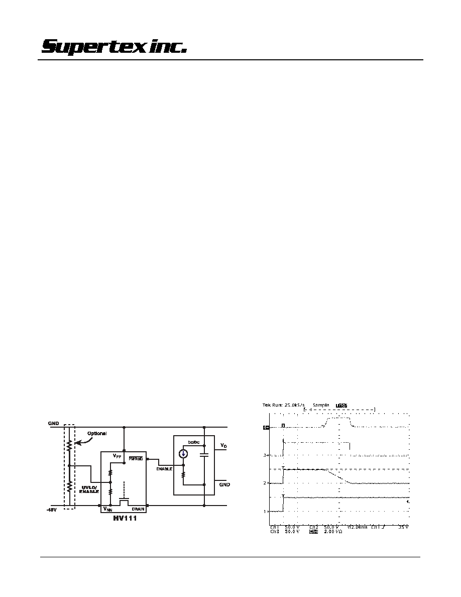
Figure 5
-
PWRGD Enable
UVLO/
Enable
V
NN
V
PP
DRAIN
PWRGD
GND
optional
ENABLE
DC/DC
GND
V
O
HV111
-48V
T
4

HV111
Thermal Shutdown
Auto-Retry
In addition to the above parameters, the HV111 will
shutdown if the temperature on the die reaches ~135∞C and
it will not restart until the temperature drops to 100∞C or less
(could be significantly less). The thermal sensor is key in
providing a bullet proof power management solution
because it ensures that the device will turn off long before
damage can occur. This is a significant advantage over
solutions that do not contain an integral MOSFET as then
the temperature cannot be easily sensed quickly and
accurately.
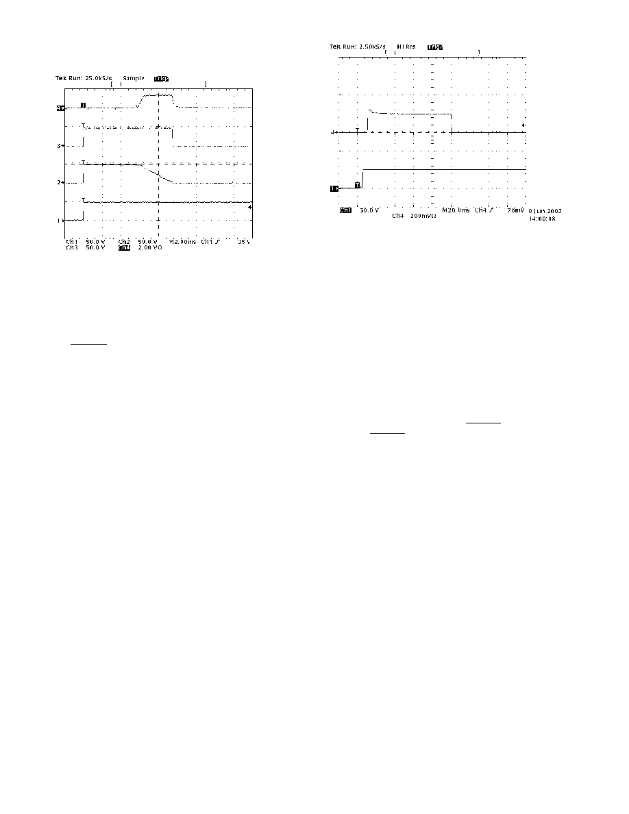
Any fault condition will cause an automatic 9sec retry to
occur. This retry will occur indefinitely (as long as the
thermal supervisor is satisfied). Figure 6 shows typical
waveforms for the auto-retry.
50V/div
200ma/div
PWRGD
V
PP
-V
NN
I
DS
Thermal engineering using the HV111 is key to proper
system operation. The 1
MOSFET pass element may
reach a value as high as 1.5
at high temperatures. There
are numerous methods to reduce the thermal resistance of
the R
JA
. The following table describes some options:
Method
R
JA
Description
FR4 70-80∞
C/W
Straight
Convection
FR4 Heat Sink
40∞ C/W
10cm
2
PCB H/S
FR4 + H/S
13∞ C/W
External Sink + Holes
IMS (40cm
2
)
9∞ C/W
Floating in Air
IMS* w/ H/S
4.5∞ C/W
External Heatsink
Timers
* IMS is a metal substrate board
The timer subsystems are critical to successful operation of
the HV111. Timers are as follows:
To determine your required thermal impedance, R
JA
, is quite
simple. In a parallel to Ohms law, Power x
R
JA
=
T.
Junction temperature, which is limited to 120
∞
C minimum, is
Tmaxambient +
T. For example, if the highest operating
ambient temperature were 55
∞
C as with many networking
applications, and the current were 1.6A, then the required
thermal resistance would be calculated as follows:
Timer Duration
Power-on-Reset
1
4.5ms
Initial Inrush Timeout
2
75ms
Shorted Inrush PWM
10
µ
s
Shorted Circuit Timer
75ms
Second Inrush (Diode
`OR'ing):
Return to Limit
Timeout
10
µ
s
(100
µ
s)
3
75ms
Auto-Retry 9sec
Determine maximum ambient = 55
∞
C.
Determine max junction temp. = 120
∞
C
1
.
Determine max operating current = 1.6A.
Therefore
T = 120-55
∞
C = 65
∞
C.
1
This is the time from satisfying the undervoltage comparator. Each "bounce" will reset this
timer & therefore observed delay may be higher than this "ideal" delay.
Max. Power
2
= 1.23A
2
*1.5
= 3.84W.
Now
T / Power = R
JA
= 65
∞
/3.84W = 20
∞
C/W.
2
Shorted-circuit timer starts after POR timer. If V
DS
drops more than º(V
PP
-V
NN
) after t
SC
then a shorted-circuit condition exists.
To achieve a R
JA
of 20
∞
C/W or better the table above shows
that it will be necessary to use a DPAK external heatsink or
IMS substrate.
3
Limit within 10
µ
s, but may take up to 100
µ
s to settle.
Current Sensing ≠ No R
SENSE
Required
1
This is the minimum value of the low to high thermal shutdown according to the electrical
specifications on pg. 2.
2
This is the maximum MOSFET on resistance at high temperature.
The HV111 uses an internal 6000:1 current mirror to
eliminate the need for a sense resistor. This saves energy
and eliminates the need for a power component. The current
mirror used by Supertex is unique in that it utilizes special
circuitry to normalize for the variations in V
DS
between the
primary pass element and the internal element which would
otherwise cause current mismatch ≠ and forces competitors
to use internal sense resistors in similar applications. This
mechanism also provides the shorted circuit PWM
functionality which can help protect systems in the case of
severe short circuits.
5

HV111
Fast Clamp
Any MOSFET includes parasitic capacitances Ciss and Cfb.
Until power is available and the HV111 initializes, these
parasitic capacitances form a capacitor divider which will
apply to the gate the ratio of Cfb/(Ciss+Cfb)*V
PP
until the
chip is initialized. To combat this the HV111 includes a fast
acting clamp which will hold off the pass element if it sees
voltage applied on the gate of the internal pass element
even before the HV111 has initialized.
During power-up, the HV111 provides an inrush limiting
current that supplies both the load capacitor and the static
load. If the static load current is too high, not enough current
will be available to charge the capacitor before the inrush
breaker trips and disconnects the load.
PWM Current Limit (PWM I
limit
)
200ma/div
V
PP
-V
NN
I
DS
1V
Inrush Breaker Trip
V
LO
AD
0V
40ms
V
o
l
t
a
g
e
Time
1.2A limiting current
230mA
limiting
current
0ms
æ(V
PP
-V
NN
)
Figure 7 ≠ Shorted PWM I
limit
Figure 8 ≠ Inrush Breaker Timing
The HV111 includes a unique protection mode not found in
other hotswap controllers. This protection mode is directed
towards severe faults ≠ faults in which the DRAIN voltage is
unable to move more than ~1V from V
PP
.
To prevent the inrush breaker from tripping, load voltage
(V
LOAD
) must exceed æ(V
PP
-V
NN
) within 40ms. The rate at
which V
LOAD
ramps up is determined by the current available
to charge the load capacitor (after the static load current is
subtracted from the HV111's inrush limiting current). Inrush
limiting initially is 230mA until load voltage exceeds 1V, at
which point it becomes 1.2A. Thus to prevent the inrush
breaker from tripping, the following equation must be
satisfied. Note that the static load cannot exceed 230mA.
If such a shorted condition exists then the current will be
limited as shown in Figure 7 above (where the upper
waveform is the ~230mA PWM current and the lower
waveform is the input voltage). Reducing the current under
severe shorts overcomes thermal cycling in which the
HV111 turns on and off as it heats up and cools down in a
severe fault (limiting the current successively to 1.2A until
overheat). It also protects downstream systems by relieving
them of the requirement to handle the 1.2A.
(
)
3
1V
1 V
4
40ms
230mA
1.15A
PP
NN
LOAD
STATIC
STATIC
V
V
C
I
I
-
-
+
<
-
-
Although this protection is extremely helpful in the case of a
severe fault condition, it does put a limit on the charging
current available for static loads.
This equation holds as long as the static load is a constant
current. If the static load is a resistance, the equation is a
little more complicated.
A special case exists when an always-on (static) load is
present at power-up.
(
)
3
1V
1 V
4
ln 1
ln 1
40ms
230mA
1.15A
lV
PP
NN
LOAD
LOAD
LOAD
LOAD
V
V
R
C
R
R
-
-
-
+
-
<
-
6
HV111
Description of Operation
I
DS
I
DS
V
PGRND
-V
NN
V
DRAIN
-V
NN
V
DRAIN
-V
NN
V
PP
-V
NN
Figure 10 ≠ Limit Timeout
Initial Inrush Timeout
Figure 9 ≠ Turn on Waveforms
The HV111 monitors the drain source voltage and the output
current. During hotswap if the drain source does not drop
below 1/4 of input voltage within a shorted-circuit timer
period (t
SC
= 75ms), then the part will conclude that a short
circuit condition exists, will turn off the internal MOSFET and
auto-retry with a period of 9.0sec. This case is illustrated in
Fig. 10 above (where waveform 4 is DRAIN current and
waveform 1 is V
PP
). Note that if the short circuit is low
enough impedance to hold the DRAIN voltage within ~1V of
V
PP
then the PWM current limit will engage as shown in Fig.
7. Further, the PWM current limit will remain until
V
PP
≠ V
DS
>~1V.
Referring to Figure 9, the operation of the HV111 may be
illustrated. On initial power application (waveform 1 in
Fig. 9) the HV111 provides a regulated supply for the
internal circuitry. Until the proper internal voltage is achieved
all circuits are held reset, the N-channel MOSFET is off and
the PWRGD bar pin is open (INACTIVE). Once the internal
regulator is safe to operate, the under voltage lock out
(UVLO) senses the input voltage. The UVLO will hold the
pass element off until it is satisfied. At any time during the
start up cycle or thereafter, the input voltage falling below
the UVLO threshold will turn off the N-channel MOSFET and
reset all internal circuitry. The IC also includes a clamp for
the spurious inrush through Cload and the Cfb of the
MOSFET pass element. A normal restart sequence will be
initiated once the input voltage rises above the UVLO
threshold.
After the hotswap period is finished successfully, the internal
MOSFET is turned fully on & the PWRGD bar is pulled low
(ACTIVE). PWRGD bar operation (connected to a pullup) is
illustrated by Waveform 3 in Fig. 9.
The UVLO supervisor works in conjunction with a power on
reset (POR) timer. The timer is approximately 4.5ms to
overcome contact bounce. During the contact bounce if
input voltage falls below the UVLO threshold voltage then
the POR timer will reset. In this way the card will be held off
until bouncing ends. The POR timer will restart again when
the input voltage rises above the UVLO threshold once
again. After a full POR period is satisfied, the N-channel
MOSFET begins to turn on to charge the output capacitor
with a current source limited to ~1.2A (illustrated by
Waveform 4 in Fig. 9). Note the PWM protection at the
leading edge of the current rise in Waveform 4; this is the
PWM protection limiting current because a capacitor initially
appears as a dead short. Waveform 2 shows the V
DS
or
DRAIN pin.
7

HV111
Circuit Breaker/Fast Return to
Limit (Diode `OR'ing)
Fast return to limit also acts as a circuit breaker with delay,
in that large currents will be limited and then the system shut
down if it does not recover. Keep in mind, however, that
severe faults which bring V
DRAIN
within ~1V of V
PP
will be
limited with the PWM Ilimit function. Fast return to limit also
overcomes the problem of "second inrush" or "diode `OR'ing
which is illustrated in Fig. 12 above. To understand this
phenomenon, consider what happens when the system has
been operating from the battery from a length of time. The
battery voltage has dropped perhaps ten volts or more.
Suddenly power is restored and the voltage suddenly jumps
from the battery voltage to the fully regulated input voltage.
This voltage jump puts a dv/dt upon the filter capacitances
that creates a second inrush. This second inrush can cause
damage if not limited, which is the purpose of the second
inrush fast return to limit.
V
PWRGD
-V
NN
I
DS
1A/div
V
DRAIN
-V
NN
Test Setup
I
16" Long
V
IN
3" Long
12" Long
Resistive
Load Box
Cload
100
µ
f
100k
V_PWRGD
Vds
GND
Current Probe
Iin
48V
DC Source
C_Source
470
µ
f
+
≠
PWRGD
Drain
Figure 11 ≠ Fast Return to Limit
A current monitor continually examines the current level
(waveform 4 in Fig. 10 & 11) and if it exceeds 2A at any
time, the MOSFET changes to a fixed 1.2A current source.
The MOSFET will remain in this state until the expiration of
an over-current timer (t
OC
= 75ms), whereafter the MOSFET
gate will be turned off and 9sec auto-retry interval will begin
(see DRAIN waveform 2 in Fig. 11, waveform 3 is V
PP
). In
the event that the over-current is cleared before the over-
current timer has expired, then the over-current timer will be
reset.
The 2A breaker will react and begin to limit current in under
10
µ
s, however, it may take up to 100
µ
s for the system to
stabilize at the limit level (1.2A).
UVLO/
Enable
V
NN
V
PP
DRAIN
PWRGD
GND
optional
ENABLE
DC/DC
GND
V
O
HV111
-48V
BAT
Figure 12 ≠ Diode `OR'ing
8

HV111
Package Information
7/24/03
9
Supertex inc.
2003 Supertex Inc. All rights reserved. Unauthorized use ofr reproduction prohibited.
1225 Bordeaux Drive, Sunnyvale, CA 94089
TEL: (408) 222-8888 ∑ FAX: (408) 222-4895
www.supertex.com