 | –≠–ª–µ–∫—Ç—Ä–æ–Ω–Ω—ã–π –∫–æ–º–ø–æ–Ω–µ–Ω—Ç: HV62208PG | –°–∫–∞—á–∞—Ç—å:  PDF PDF  ZIP ZIP |

1
HV62208
32-Channel 256 Gray-Shade High Voltage Driver
Absolute Maximum Ratings
Supply voltage, V
DD
-0.5V to +7.5V
Supply voltage, V
PP
-0.5V to +80V
Supply voltage, V
NN
-15V to 0V
Logic input levels
-0.5 to V
DD
+ 0.5V
Continuous total power dissipation
1.2W
Operating temperature range
-40
∞
C to +85
∞
C
Storage temperature range
-65
∞
C to +150
∞
C
Notes:
All voltages are referenced to GND.
Maximum V
PP
to V
NN
voltage is 90V.
For operation above 25
∞
C ambient derate linearly to 85
∞
C at 20mW/
∞
C.
Features
HVCMOS
Æ
technology
5V CMOS inputs
Up to 80V output voltage
PWM gray shade conversion
Capable of 256 levels of gray shading
Balanced shift clock complies with RS-422
8MHz shift and count clock frequency
16MHz data throughput rate
8 bit data bus
32 outputs per device
BLANK function
General Description
Not recommended for new designs. Please use HV632 instead.
The HV622 is a 32-channel gray-shade column driver IC de-
signed for driving electrofluorescent displays. Using Supertex's
unique HVCMOS
Æ
technology, it is capable of 256 levels of gray
shading by PWM conversion.
The shift clock is a balanced clock with electrical characteristics
complying with EIA RS-422 standard. Input data, in groups of
eight, is latched into a set of data latches on both edges of the shift
clock. The data shifted in the first data latch corresponds to
HV
OUT
1, the second data latch corresponds to HV
OUT
2, and so on.
These data are compared to the contents of the master binary
counter which counts on both edges of the count clock. Each time
the master counter begins to decrement from 1111 1111, the data
in the data latches are compared with the contents of the counter;
if they match, the corresponding outputs will go high. The master
counter counts down to 0000 0001 and then starts to count up
again. The outputs that are at high will stay at high until the
contents of the counter match the data in the data latches again.
Therefore, the higher the binary data in the data latches, the
longer the outputs will stay at high. Thus, different high voltage
pulse widths are produced. When the counter reaches its
1111 1111 count while counting up, the device is ready for the
next operation cycle. A data value of 0000 0000 produces no
pulse; the output stays low.
The BLANK input signal will reset the master counter to all ones
(1111 1111) and set all high voltage outputs to low.
02/96/022
Supertex Inc. does not recommend the use of its products in life support applications and will not knowingly sell its products for use in such applications unless it receives an adequate "products liability
indemnification insurance agreement." Supertex does not assume responsibility for use of devices described and limits its liability to the replacement of devices determined to be defective due to
workmanship. No responsibility is assumed for possible omissions or inaccuracies. Circuitry and specifications are subject to change without notice. For the latest product specifications, refer to the
Supertex website: http://www.supertex.com. For complete liability information on all Supertex products, refer to the most current databook or to the Legal/Disclaimer page on the Supertex website.
Ordering Information
Package Option
Device
64-Lead 3-Sided Plastic Gullwing
Die
HV62208
HV62208PG
HV62208X
2
Electrical Characteristics
(Over recommended conditions of V
DD
= 5V, V
PP
= 70V, V
NN
= -10V, T
A
= 25
∞
C unless otherwise noted)
HV62208
Symbol
Parameter
Min
Max
Units
Conditions
V
DD
Low-voltage digital supply voltage
4.5
5.5
V
I
DD
V
DD
supply current
25
mA
f
SC
= 8MHz, f
CC
= 8MHz
I
DDQ
Quiescent V
DD
supply current
100
µ
A
All V
IN
= GND, Count Clock = V
DD
I
IH
High-level input current
10
µ
A
V
IN
= V
DD
I
IL
Low-level input current
-10
µ
A
V
IL
= GND
I
OH
High-level output current
-1.0
mA
I
OL
Low-level ouptut current
1.0
mA
Symbol
Parameter
Min
Max
Units
Conditions
f
SC
Shift clock frequency
8.0
MHz
f
CC
Count clock frequency
8.0
MHz
f
DIN
Data In frequency
16
MHz
t
CW
Chip select pulse width
80
ns
t
CSS
Chip select to shift clock set-up time
15
ns
t
CSH
Chip select to shift clock hold time
45
ns
t
SCC
Shift clock cycle time
125
ns
t
DSS
Data to shift clock set-up time
10
ns
t
DSH
Data to shift clock hold time
52
ns
t
DW
Data In pulse width
62
ns
t
LCW
Load count pulse width
75
ns
t
CCW
Count clock pulse width
62.5
ns
t
CCC
Count clock cycle time
125
ns
t
LCD
Load count to count clock delay
100
ns
t
CCD
Count clock to HV
OUT
turn-on/turn-off
600
ns
C
L
= 15pF
t
BLW
BLANK pulse width
700
ns
t
BLD
BLANK to HV
OUT
delay
500
ns
C
L
= 15pF
t
CDD
Count clock delay between count down and
500
ns
count up cycles
Symbol
Parameter
Min
Max
Units
Conditions
I
PPQ
Quiescent V
PP
supply current
100
µ
A
All HV
OUT
low or high
I
OUT(p)
P-channel output current
-4.0
mA
I
OUT(n)
N-channel output current
4.0
mA
Symbol
Parameter
Min
Max
Units
Conditions
V
DD
Low-voltage analog supply voltage
4.5
5.5
V
I
DD
V
DD
supply current
100
µ
A
f
SC
= 8MHz, f
CC
= 8MHz
I
DDQ
Quiescent V
DD
supply current
100
µ
A
All V
IN
= GND, Count Clock = V
DD
Low-Voltage DC Characteristics (Digital)
Low-Voltage DC Characteristics (Analog)
High-Voltage DC Characteristics
AC Characteristics

3
V
DD
Input
GND
V
PP
V
NN
HV
OUT
Logic Inputs
GND
Data Out
Logic Data Output
High Voltage Output
V
DD
Symbol
Parameter
Min
Max
Units
Conditions
V
DD
Logic supply voltage
4.5
5.5
V
V
PP
Positive high-voltage supply
12
70
V
V
NN
Negative high-voltage supply
-8
-10
V
V
IL
Low-level input voltage
0
1
V
V
IH
High-level input voltage
V
DD
≠1
V
DD
V
f
SC
Shift clock frequency
8
MHz
f
CC
Count clock frequency
8
MHz
T
A
Operating temperature
-40
+85
∞
C
Recommended Operating Conditions
HV62208
Input and Output Equivalent Circuits
Pin #
Name
I/O
Function
27-30
D1 ≠ D8
I
Inputs for binary-format parallel data
36-29
(D8 is the most significant bit)
34
Shift Clock
I
Triggers data on both edges
35
Shift Clock
I
Triggers data on both edges
31
Count Clock
I
Input to the counter
24
CSI
I
Chip select input to enable the device to accept data
25
CSO
O
Chip select output to enable the next device
33
Load Count
I
Input to initiate the counting
26
Blank
I
Input to reset the counter and HV
OUT
4-19
HV
OUT
1
≠ HV
OUT
32
O
High-voltage outputs
46-61
23,43
V
PP
--
Positive high-voltage supply
41
V
DD
(Analog)
--
Low-voltage analog supply voltage
40
V
DD
(Digital)
--
Low-voltage digital supply voltage
22,44
V
NN
--
Negative high-voltage supply
20-21
GND (Digital)
--
Digital ground
42
GND (Analog)
Analog ground
Pin Definitions

4
HV
OUT
Shift
Clock
1
2
3
4
16
VALID DATA
1
2
3
4
16
CSI
CSO
LC
Count
Clock
1
1
252
253
254
255
255
254
253
252
1
1
252
253
254
255
255
254
253
252
VALID DATA
Data
Latch 1
Comparator
& Latch 1
L/T
>
8
8
Data
Latch 2
Comparator
& Latch 2
L/T
>
8
8
Data
Latch 3
Comparator
& Latch 3
L/T
>
8
8
Data
Latch 32
Comparator
& Latch 32
L/T
>
8
Logic
8 Bit
Counter
>
8
HV
OUT
1
HV
OUT
2
HV
OUT
3
HV
OUT
32
∑
∑
∑
V
PP
V
PP
8 Bit
Data In
8
>
>
>
>
>
Count
Clock
Blank
L/T = Level Translator
CSO
CSI
V
NN
Logic
Logic
Logic
Logic
>
V
NN
>
Load
Count
+
≠
Shift Clock
Shift
Clock
Functional Block Diagram
HV62208
Timing Diagrams

5
HV62208
Timing Diagrams
t
CW
t
CSS
DATA
SET 1
t
DSS
t
DSH
t
DW
LOADING LAST DEVICE
NEXT LOADING CYCLE
CSI
Shift
Clock
Load
Count
Count
Clock
Count
Clock
HV
OUT
t
SCC
SC1
50%
t
CSH
50%
50%
SC2
SC16
SC1
SCN
DATA
SET 2
DATA
SET 3
DATA
SET 31
DATA
SET 32
DATA
SET 1
t
LCW
t
CCW
t
CCC
t
LCD
V
IH
V
IL
V
IH
V
IL
V
IH
V
IL
V
IH
V
IL
V
IH
V
IL
50%
50%
90%
10%
10%
50%
50%
50%
50%
t
CCD
DATA
SET 2
DATA
SET 2N -1
BLANK
t
BLW
t
CDD
V
IH
V
IL
50%
50%
255
254
3
3
2
2
1
1
90%
HV
OUT
t
BLD
V
PP
V
NN
V
IL
50%
50%
V
IH
Data
1≠8
V
PP
V
NN
DATA
SET 2N
50%
90%
t
CCD

6
1235 Bordeaux Drive, Sunnyvale, CA 94089
TEL: (408) 744-0100 ∑ FAX: (408) 222-4895
www.supertex.com
02/06//02
©2002 Supertex Inc. All rights reserved. Unauthorized use or reproduction prohibited.
Index
1
24
64
41
25
40
top view
3-sided Plastic 64-pin Gullwing Package
Package Outline
HV62208
Pin Configurations
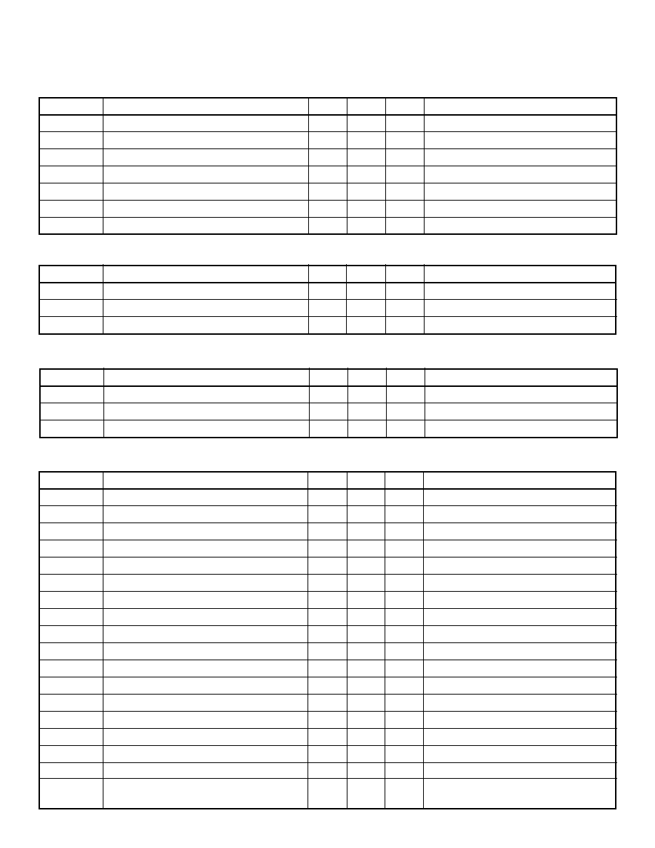
Pin
Function
1
N/C
2
N/C
3
N/C
4
HV
OUT
17
5
HV
OUT
18
6
HV
OUT
19
7
HV
OUT
20
8
HV
OUT
21
9
HV
OUT
22
10
HV
OUT
23
11
HV
OUT
24
12
HV
OUT
25
13
HV
OUT
26
14
HV
OUT
27
15
HV
OUT
28
16
HV
OUT
29
17
HV
OUT
30
18
HV
OUT
31
19
HV
OUT
32
20
GND (Digital)
21
GND (Digital)
22
V
NN
23
V
PP
24
CSI
25
CSO
26
Blank
27
D1
28
D2
29
D3
30
D4
31
Count Clock
32
N/C
Pin
Function
33
Load Count
34
Shift Clock
35
Shift Clock
36
D5
37
D6
38
D7
39
D8
40
V
DD
(Digital)
41
V
DD
(Analog)
42
GND (Analog)
43
V
PP
44
V
NN
45
N/C
46
HV
OUT
1
47
HV
OUT
2
48
HV
OUT
3
49
HV
OUT
4
50
HV
OUT
5
51
HV
OUT
6
52
HV
OUT
7
53
HV
OUT
8
54
HV
OUT
9
55
HV
OUT
10
56
HV
OUT
11
57
HV
OUT
12
58
HV
OUT
13
59
HV
OUT
14
60
HV
OUT
15
61
HV
OUT
16
62
N/C
63
N/C
64
N/C