 | –≠–ª–µ–∫—Ç—Ä–æ–Ω–Ω—ã–π –∫–æ–º–ø–æ–Ω–µ–Ω—Ç: HV632X | –°–∫–∞—á–∞—Ç—å:  PDF PDF  ZIP ZIP |
1
HV632
07/08/03
Supertex Inc. does not recommend the use of its products in life support applications and will not knowingly sell its products for use in such applications unless it receives an adequate "products liability
indemnification insurance agreement." Supertex does not assume responsibility for use of devices described and limits its liability to the replacement of devices determined to be defective due to
workmanship. No responsibility is assumed for possible omissions or inaccuracies. Circuitry and specifications are subject to change without notice. For the latest product specifications, refer to the
Supertex website: http://www.supertex.com. For complete liability information on all Supertex products, refer to the most current databook or to the Legal/Disclaimer page on the Supertex website.
32-Channel 256 Gray-Shade High Voltage Driver
Features
HVCMOS
Æ
technology
5V CMOS inputs
Up to 80V output voltage
PWM gray shade conversion
Capable of 256 levels of gray shading
10MHz shift and count clock frequency
20MHz data throughput rate
8 bit data bus
32 outputs per device
BLANK function
Output polarity control
General Description
The HV632 is a 32-channel gray-shade column driver IC de-
signed for driving electrofluorescent displays. Using Supertex's
unique HVCMOS
Æ
technology, it is capable of 256 levels of gray
shading by PWM conversion.
Input data, in groups of eight, is latched into a set of data latches
on both edges of the shift clock. The data shifted in the first data
latch corresponds to HV
OUT
1, the second data latch corresponds
to HV
OUT
2, and so on. These data are compared to the contents
of the master binary counter which counts on both edges of the
count clock. Each time the master counter begins to decrement
from 1111 1111, the data in the data latches are compared with
the contents of the counter; if they match, the corresponding
outputs will go high. The master counter counts down to 0000
0001 and then starts to count up again. The outputs that are at
high will stay at high until the contents of the counter match the
data in the data latches again. Therefore, the higher the binary
data in the data latches, the longer the outputs will stay at high.
Thus, different high voltage pulse widths are produced. When
the counter reaches its 1111 1111 count while counting up,
the device is ready for the next operation cycle. A data value of
0000 0000 produces no pulse; the output stays low.
The BLANK input signal will reset the master counter to all ones
(1111 1111) and set all high voltage outputs to low, or will set all
high voltage outputs to high state, when the POL is low. The POL
input signal, forced low, will invert the polarity of the output pulse.
If left unconnected, POL input will be pulled high to V
DD
by an on-
chip resistor.
Applications
Field Emission Displays (FED)
Polymer Liquid Crystal Displays (PLCD)
Vacuum Fluorescent Displays (VFD)
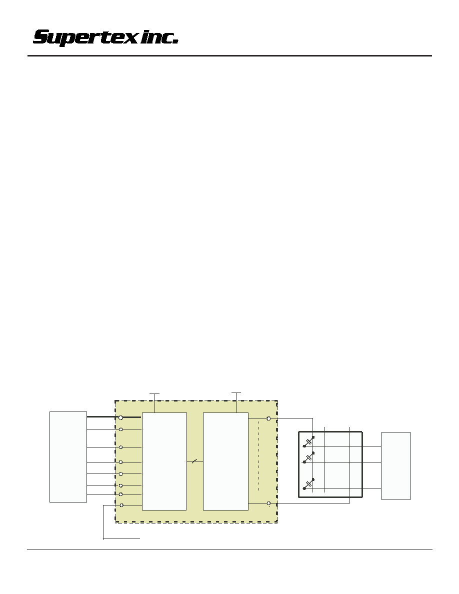
DIN(1-8)
SC
CSO
CSI
LC
BL
CC
Shift Register
Latches
Counter
Compar ators
Low Voltage
High Voltage
HVout1
HVout32
Micro
Processor
Scan
Driver
HV57908
Colunms
(Cathodes)
Display
Panel
(FED)
Supertex HV632
CSI
Level
Translators
&
Push-Pull
Output
Buffers
POL
High Voltage
Power Supply
Low Voltage
Power Supply
32
for cascading the next HV632
HV632
Initial Release
Typical Application

2
HV632
Ordering Information
Package Option
Device
64-Lead 3-Sided Plastic Gullwing
Die
HV632
HV632PG
HV632X
Absolute Maximum Ratings
Supply voltage, V
DD
-0.5V to +7.5V
Supply voltage, V
PP
-0.5V to +90V
Logic input levels
-0.5 to V
DD
+ 0.5V
Continuous total power dissipation
1.2W
Operating temperature range
-40
∞
C to +85
∞
C
Storage temperature range
-65
∞
C to +150
∞
C
Notes:
All voltages are referenced to GND.
For operation above 25
∞
C ambient derate linearly to 85
∞
C at 20mW/
∞
C.
Electrical Characteristics
(Over recommended conditions of V
DD
= 5V, V
PP
= 80V, T
A
= 25
∞
C unless otherwise noted)
Symbol
Parameter
Min
Max
Units
Conditions
V
DD
Low-voltage digital supply voltage
4.5
5.5
V
I
DD
V
DD
supply current
25
mA
f
SC
= 10MHz, f
CC
= 10MHz
I
DDQ
Quiescent V
DD
supply current
150
µ
A
All V
IN
= GND, Count Clock = V
DD
I
IH
High-level input current
10
µ
A
V
IN
= V
DD
I
IL
Low-level input current
-10
µ
A
V
IL
= GND
I
OH
High-level output current
-1.0
mA
V
OUT
=0.9 V
DD
I
OL
Low-level ouptut current
1.0
mA
V
OUT
=0.1 V
DD
Low-Voltage DC Characteristics (Digital)
Symbol
Parameter
Min
Max
Units
Conditions
I
PPQ
Quiescent V
PP
supply current
100
µ
A
All HV
OUT
low or high
I
OUT(p)
P-channel output current
-4.0
mA
HV
OUT
=75V
I
OUT(n)
N-channel output current
4.0
mA
HV
OUT
=5V
I
PP
V
PP
supply current
1.1
mA
C
L
=0pF, F
CC
=10Mhz
High-Voltage DC Characteristics

3
HV632
Electrical Characteristics
(Over recommended conditions of V
DD
= 5V, V
PP
= 80V, T
A
= 25
∞
C unless otherwise noted)
Symbol
Parameter
Min
Max
Units
Conditions
f
SC
Shift clock frequency
10
MHz
f
CC
Count clock frequency
10
MHz
f
DIN
Data In frequency
20
MHz
t
CW
Chip select pulse width
80
ns
t
CSS
Chip select to shift clock set-up time
5.0
ns
t
CSH
Chip select to shift clock hold time
15
ns
t
SCC
Shift clock cycle time
100
ns
t
DSS
Data to shift clock set-up time
10
ns
t
DSH
Data to shift clock hold time
40
ns
t
DW
Data In pulse width
50
ns
t
LCW
Load count pulse width
75
ns
t
CCW
Count clock pulse width
50
ns
t
CCC
Count clock cycle time
100
ns
t
LCD
Load count to count clock delay
100
ns
t
CCD
Count clock to HV
OUT
turn-on/turn-off
300
ns
C
L
= 15pF
t
BLW
BLANK pulse width
700
ns
t
BLD
BLANK to HV
OUT
delay
500
ns
C
L
= 15pF
t
CDD
Count clock delay between count down and
150
ns
count up cycles
t
CSOH
CSO delay output for High
40
ns
C
L
=15pF
t
CSOL
CSO delay output for Low
40
ns
C
L
=15pF
AC Characteristics
Symbol
Parameter
Min
Max
Units
Conditions
V
DD
Logic supply voltage
4.5
5.5
V
V
PP
Positive high-voltage supply
12
80
V
V
IL
Low-level input voltage
0
1
V
V
IH
High-level input voltage
V
DD
≠1
V
DD
V
T
A
Operating temperature
-40
+85
∞
C
Recommended Operating Conditions
Pin #
Name
I/O
Function
27-30
D1 ≠ D8
I
Inputs for binary-format parallel data
36-39
(D8 is the most significant bit)
34
Shift Clock
I
Triggers data on both edges
31
Count Clock
I
Input to the counter
32
POL
I
Output polarity control
24
CSI
I
Chip select input to enable the device to accept data
25
CSO
O
Chip select output to enable the next device
33
Load Count
I
Input to initiate the counting
26
Blank
I
Input to reset the counter and HV
OUT
4-19
HV
OUT
1
≠ HV
OUT
32
O
High-voltage outputs
46-61
23,43
V
PP
--
Positive high-voltage supply
40
V
DD
--
Low-voltage digital supply voltage
22,44
HV
GND
--
High voltage ground
20-21
GND
--
Digital ground
Pin Definitions

4
HV632
Functional Block Diagram
Data
Latch 1
Comparator
& Latch 1
L/T
>
8
8
Data
Latch 2
Comparator
& Latch 2
L/T
>
8
8
Data
Latch 3
Comparator
& Latch 3
L/T
>
8
8
Data
Latch 32
Comparator
& Latch 32
L/T
>
8
Logic
8 Bit
Counter
>
8
HV
OUT
1
HV
OUT
2
HV
OUT
3
HV
OUT
32
∑
∑
∑
V
PP
V
PP
8 Bit
Data In
8
>
>
>
>
>
Count
Clock
Blank
L/T = Level Translator
CSO
CSI
HV
GND
Logic
Logic
Logic
Logic
>
HV
GND
>
Load
Count
Shift
Clock
POL*
* Internal pull-up resistor
5
HV632
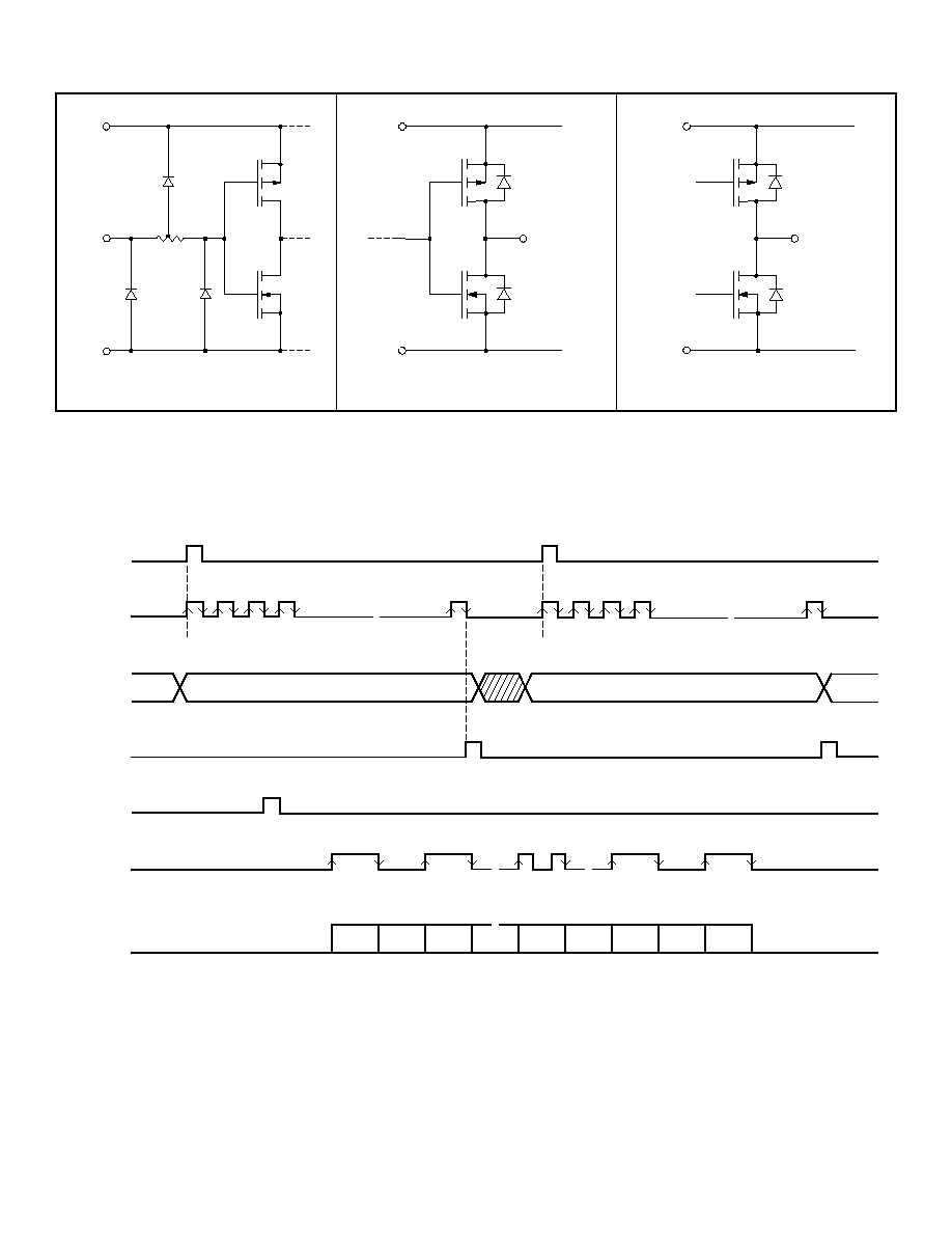
Input and Output Equivalent Circuits
V
DD
Input
GND
V
PP
HV
GND
HV
OUT
Logic Inputs
GND
Data Out
Logic Data Output
High Voltage Output
V
DD
HV
OUT
Shift
Clock
1
2
3
4
16
VALID DATA
1
2
3
4
16
CSI
CSO
LC
Count
Clock
1
1
252
253
254
255
255
254
253
252
1
1
252
253
254
255
255
254
253
252
VALID DATA
Timing Diagrams