HV850
________________________________________________________________________________
Supertex, Inc. 1/21/04
1
Initial Release
High Voltage Low Noise Inductorless EL Lamp Driver
Features
No external components required when using an
external EL clock frequency
EL frequency can be set by an external resistor
Low Noise
DC to AC converter
Drives up to 4.5nF load (approx. 2.0
2
inches)
Output voltage regulation
Enable function
Applications
Cell phone keypads and displays
Transceivers
MP3 Players
Watches
Pagers
Measuring instruments/gauges
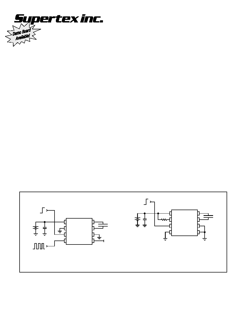
Typical Application Circuits
General Description
Supertex HV850 is a high voltage electroluminescent
(EL) Lamp Driver IC. It is designed to drive EL lamps
of up to 2.0in
2
, with capacitive values up to 4.5nF.
HV850 converts a low voltage DC input to a high
voltage AC output across an EL lamp. It uses a
charge pump scheme to boost the input voltage
eliminating the need for an external inductor, diode,
and high voltage capacitor commonly found in
conventional topologies.
The charge pump circuit discharges its energy into
an EL lamp through a high voltage H-bridge. Once
the voltage reaches its regulated limit, it is turned off
to conserve power. The EL lamp is then discharged
to ground and the H-bridge changes state to allow
the charge pump to charge the EL lamp in the
opposite direction.
The EL lamp frequency can be set either by an
external resistor R
EL
or by applying an external clock
where the clock frequency is divided by 128 to set
the EL lamp frequency.
EL lamp frequency set by an external clock
EL
Lamp
V
DD
V
B
R
EL
GND
V
A
HV850MG
EN
Clk-in
Clk-en
V
DD
=ON
GND=OFF
V
DD
GND
C
DD
V
DD
+
-
V
DD
EL
Lamp
V
DD
V
B
R
EL
GND
V
A
HV850MG
EN
Clk-in
Clk-en
V
DD
=ON
GND=OFF
C
DD
V
DD
+
-
R
EL
EL lamp frequency set by R
EL
HV850
________________________________________________________________________________
Supertex, Inc. 1/21/04
2
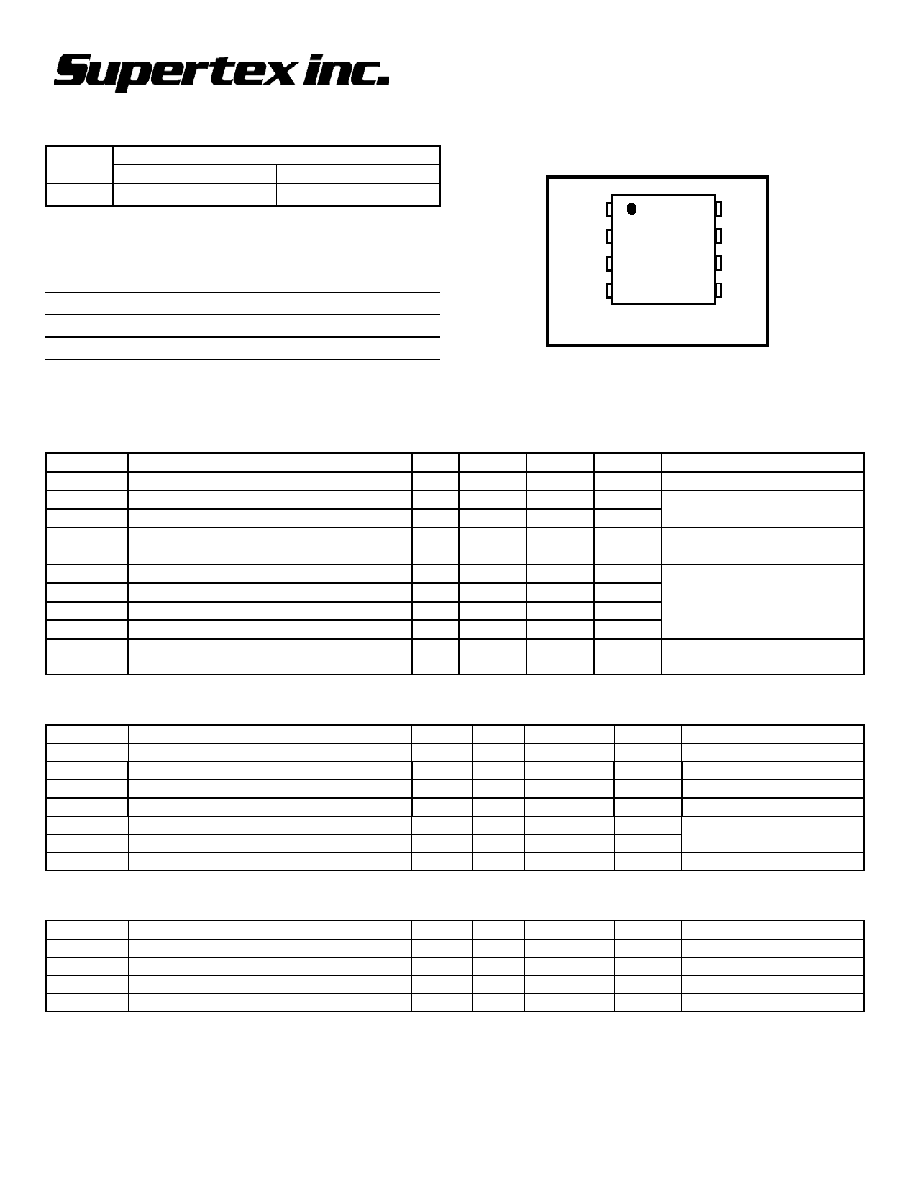
Ordering Information
Package
Device
MSOP-8 Die
HV850 HV850MG*
HV850X
Absolute Maximum Ratings*
Vdd, Supply Voltage
-0.5V to 4.5V
Operating Temperature
-25�C to +85�C
Storage Temperature
-65�C to +150�C
Power Dissipation MSOP-8
300mW
*Absolute Maximum Ratings are those values beyond which damage
to the device may occur. Functional operation under these conditions is
not implied. Continuous operation of the device at the absolute rating
level may affect device reliability. All voltages are referenced to device
ground.
Electrical Characteristics
(
unless otherwise specified: T
A
= 25
�
C, V
DD
= 3.5V)
Symbol Parameter
Min Typ
Max
Units Conditions
I
DDQ
Quiescent
current
150 nA EN=0V
V
A
or V
B
Peak output voltage
63
70
77
V
V
A
-V
B
Peak to Peak output voltage
126
140
154
V
No load.
f
EL
EL lamp frequency
225
250
275
Hz
R
EL
=1.65M
or
CLK=32KHz
I
DD
Operating
current
16 mA
V
A
or V
B
Peak output voltage
54
61
68.5
V
V
A
-V
B
Peak to Peak output voltage
110
122
134
V
f
EL
EL lamp frequency
250
294
338
Hz
See Figure 1, V
DD
=3.5V,
R
EL
=1.5M
,
Load=3.3nF+1K
t
rout
Output voltage rise time
1.5
ms
f
EL
=250Hz, 1in
2
lamp, 0V to
90% of final value
Logic Inputs
Symbol Parameter
Min Typ
Max
Units Conditions
V
IL
Input logic low voltage
0
0.5
V
V
IH
Input logic high voltage
2.0
V
DD
V
I
IL
Input logic low current
1.0
�A
I
IH
Input logic high current
1.0
�A
EN
rise
Enable input rise time (for delay turn off)
0.01
10
ms
EN
fall
Enable input fall time (for delay turn off)
10�
5
s
Using external R-C
circuit, see Figure 2.
C
in
Logic input capacitance
10
pF
Recommended Operating Conditions
Symbol Parameter
Min Typ
Max
Units Conditions
V
DD
Input
voltage
3.0
4.2
V
f
req
EL lamp frequency
50
500
Hz
C
load
EL lamp capacitance
0
3.5
nF
T
A
Operating
Temperature
-25 +85 �C
V
DD
R
EL
EN
Clk-in
V
B
GND
V
A
Clk-en
MSOP
(top View)
Pin Configuration
*Product supplied on 2500 piece Carrier Tape Reels.
HV850
________________________________________________________________________________
Supertex, Inc. 1/21/04
3
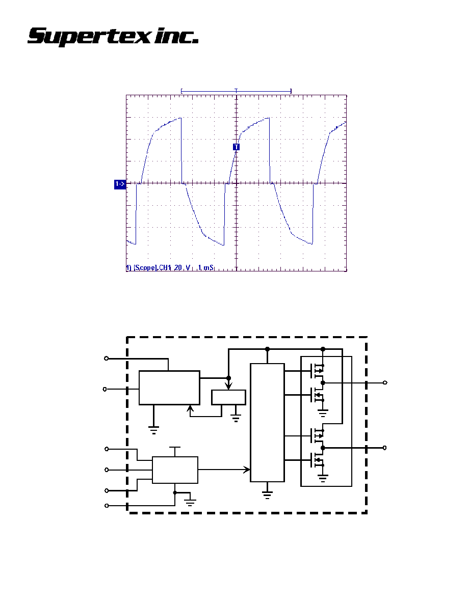
Typical Output Waveform
Vdd=3.5V, Fel=250.0Hz; Load=3.3nF+1 kohm; Idd=9.19mA, CH1 20V/div, 1mS/div
Block Diagram
Vsense
High
Voltage
Level
Trans-
lators
Capacitor
Charge Pum p
Circuit
Feedback
Vdd
MOS FET
Full Bridge
EL
Oscillator
Vdd
Rel
Clk-in
Clk-en
GND
Vdd
EN
Va
Vb
HV850
________________________________________________________________________________
Supertex, Inc. 1/21/04
4
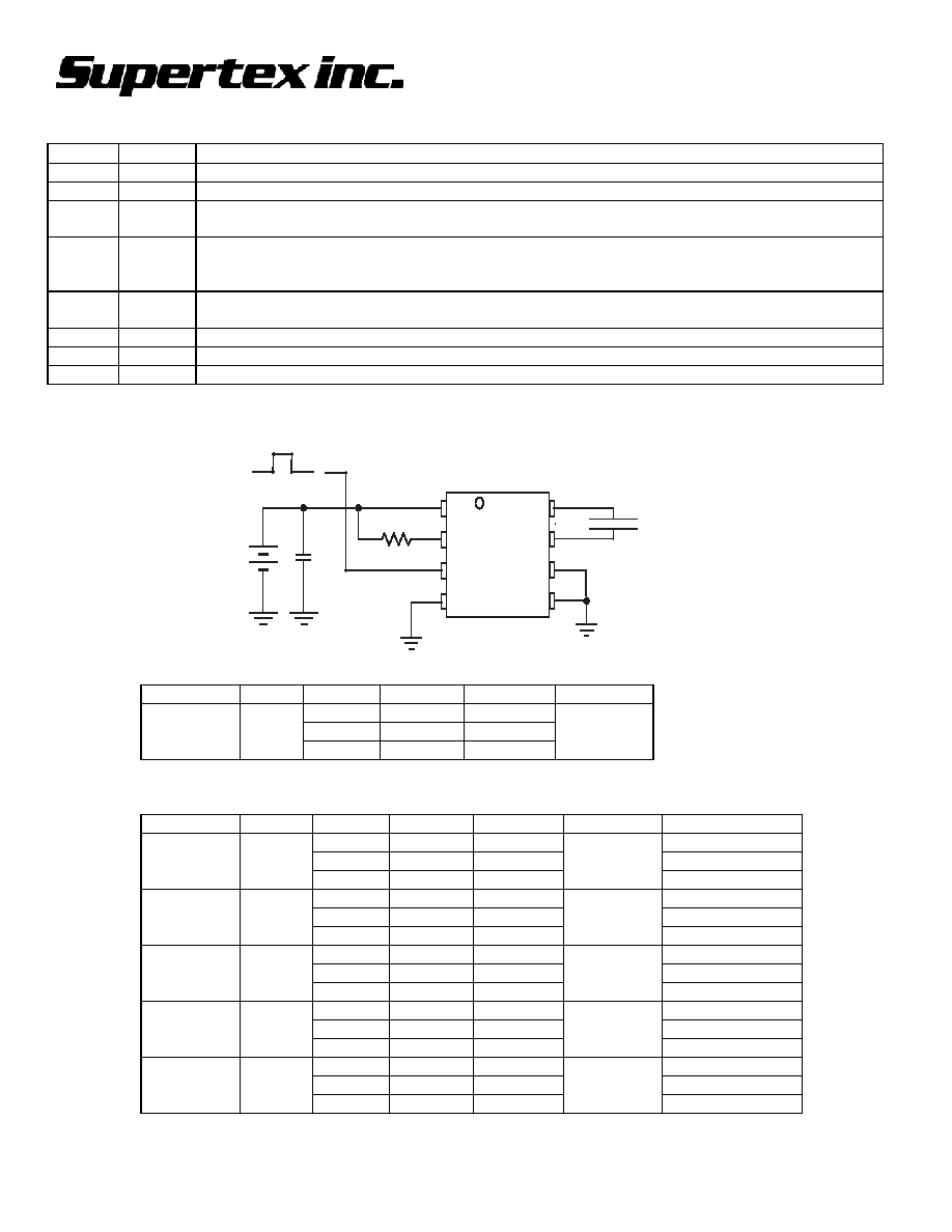
Pin Description
Pin #
Pad
Description
1 V
DD
Input supply voltage pin.
2 R
EL
An external resistor to V
DD
will set the EL lamp frequency.
3 EN
Enable input pin. Logic high will turn the device on. An external R-C circuit can be added for a
delayed turn off.
4 Clk-in
Logic input pin. An external logic clock applied to this pad can be used to set the EL lamp
frequency (see Figure 3). This is useful for applications requiring the EL lamp to be
synchronized to a system clock. Connect to ground when no in use.
5 Clk-en
Logic input pin. Logic high will cause the EL lamp frequency to be set by the Clk-in input. Logic
low will cause the EL lamp frequency to be set by the external Rel resistor.
6
Gnd
IC ground pin.
7 V
B
EL lamp driver output pin. The EL lamp is connected across V
A
and V
B
terminals.
8 V
A
EL lamp driver output pin. The EL lamp is connected across V
A
and V
B
terminals.
Figure 1: Typical Applications
Note: C
dd
=2.2
�
F, 6.3V low ESR
Load R
EL
V
DD
I
DD
Peak
V
A
f
EL
3.0V 8.9mA 53V
3.5V 10.2mA 61V
3.3nF+1K
1.5M
4.0V 10.4mA 66V
294Hz
Additional Examples
Lamp Size
R
EL
V
DD
I
DD
Peak
V
A
f
EL
Brightness
3.0V 8.4mA 53V
7.31cd/m
2
3.5V 9.4mA 62V
10.35cd/m
2
1.0in
2
1.65M
4.0V 9.9mA 66V
250Hz
12.62cd/m
2
3.0V 5.5mA 62V
11.54cd/m
2
3.5V 5.3mA 68V
14.33cd/m
2
0.5in
2
2.0M
4.0V 4.9mA 68V
210Hz
14.90cd/m
2
3.0V 5.6mA 62V
8.55cd/m
2
3.5V 5.4mA 67V
10.29cd/m
2
1.0in
2
3.3M
4.0V 5.0mA 68V
128Hz
10.94cd/m
2
3.0V 4.6mA 64V
8.25cd/m
2
3.5V 4.1mA 68V
9.62cd/m
2
0.5in
2
3.3M
4.0V 3.8mA 68V
128Hz
9.95cd/m
2
3.0V 4.8mA 64V
6.02cd/m
2
3.5V 4.4mA 68V
7.50cd/m
2
1.0in
2
4.7M
4.0V 5.0mA 68V
89Hz
10.94cd/m
2
V
DD
V
B
R
EL
GND
V
A
HV850MG
Cdd
+
-
Rel
V
DD
EN
Clk-in
Clk-en
EL
Lamp
GND=OFF
VDD=ON

HV850
________________________________________________________________________________
Supertex, Inc. 1/21/04
5
Figure 2: Push Button Turn on with Delay Turn off
Figure 3: Independent Programmable Output Frequency (f
EL
)
V
DD
V
B
R
EL
GND
V
A
HV850MG
EN
Clk-in
Clk-en
VDD
Cdd
+
-
V
DD
EL
Lamp
GND=OFF
VDD=ON
GND
EL
Lamp
Cdd
+
-
Rel
V
DD
C
R
RC time constant
will set Turn off
Delay time
Push button
turn on
V
DD
V
B
R
EL
GND
V
A
HV850MG
EN
Clk-in
Clk-en

HV850
________________________________________________________________________________
Supertex, Inc. 1/21/04
6
1/20/04natfrev15
2004 Supertex Inc. All rights reserved. Unauthorized use or reproduction prohibited.
1235 Bordeaux Drive, Sunnyvale, CA 94809
TEL: (408) 222-8888 / FAX: (408) 222-4895
www.supertex.com